Electronic assembly with carbon nanotube contact formations or interconnections

a carbon nanotube and contact formation technology, applied in the field of electromechanical assembly, can solve the problems of insufficient bonding between the die and the package substrate, and the inherently unreliable nature of the semiconductor package,

Inactive Publication Date: 2005-12-29
INTEL CORP
View PDF9 Cites 58 Cited by
  • Summary
  • Abstract
  • Description
  • Claims
  • Application Information

AI Technical Summary

Problems solved by technology

If contact formations with smaller pitches or sizes are made with modern soldering techniques, the resulting semiconductor package is inherently unreliable.
The bond between the die and the package substrate is not strong enough due to the small size of the solder ball.
Additionally, because of the small size of the solder ball (and joint) and the limited electrical and thermal conductivity of the solder, the solder balls (and / or joints) melt as the integrated circuits within the dice reach state of the art performance levels with high power outputs.
Similar problems are found with the use of metals, such as copper, for interconnects and vias which electrically connect conductive layers within the semiconductor chips.

Method used


Image

  • Electronic assembly with carbon nanotube contact formations or interconnections
  • Electronic assembly with carbon nanotube contact formations or interconnections
  • Electronic assembly with carbon nanotube contact formations or interconnections

Examples


Embodiment Construction

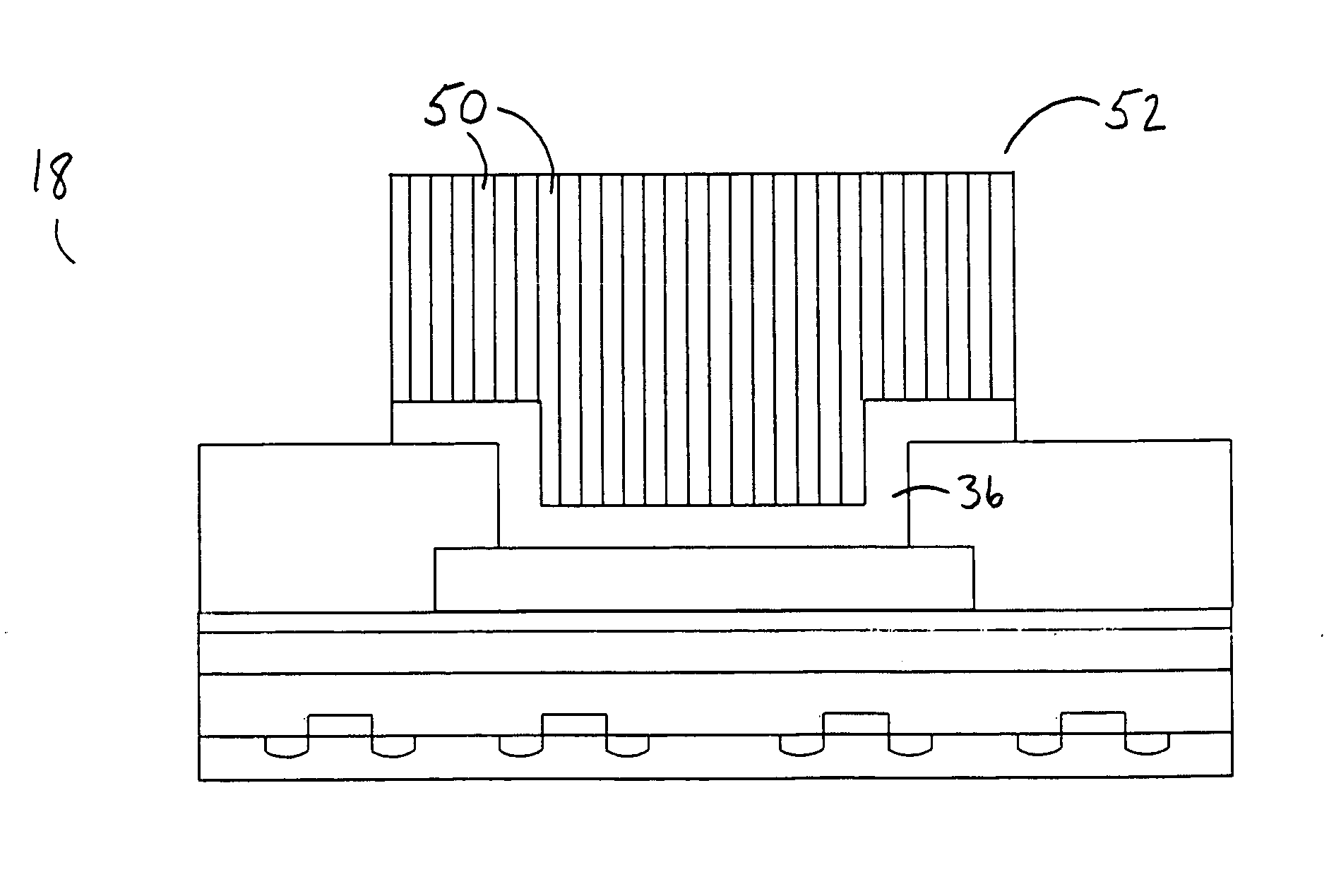
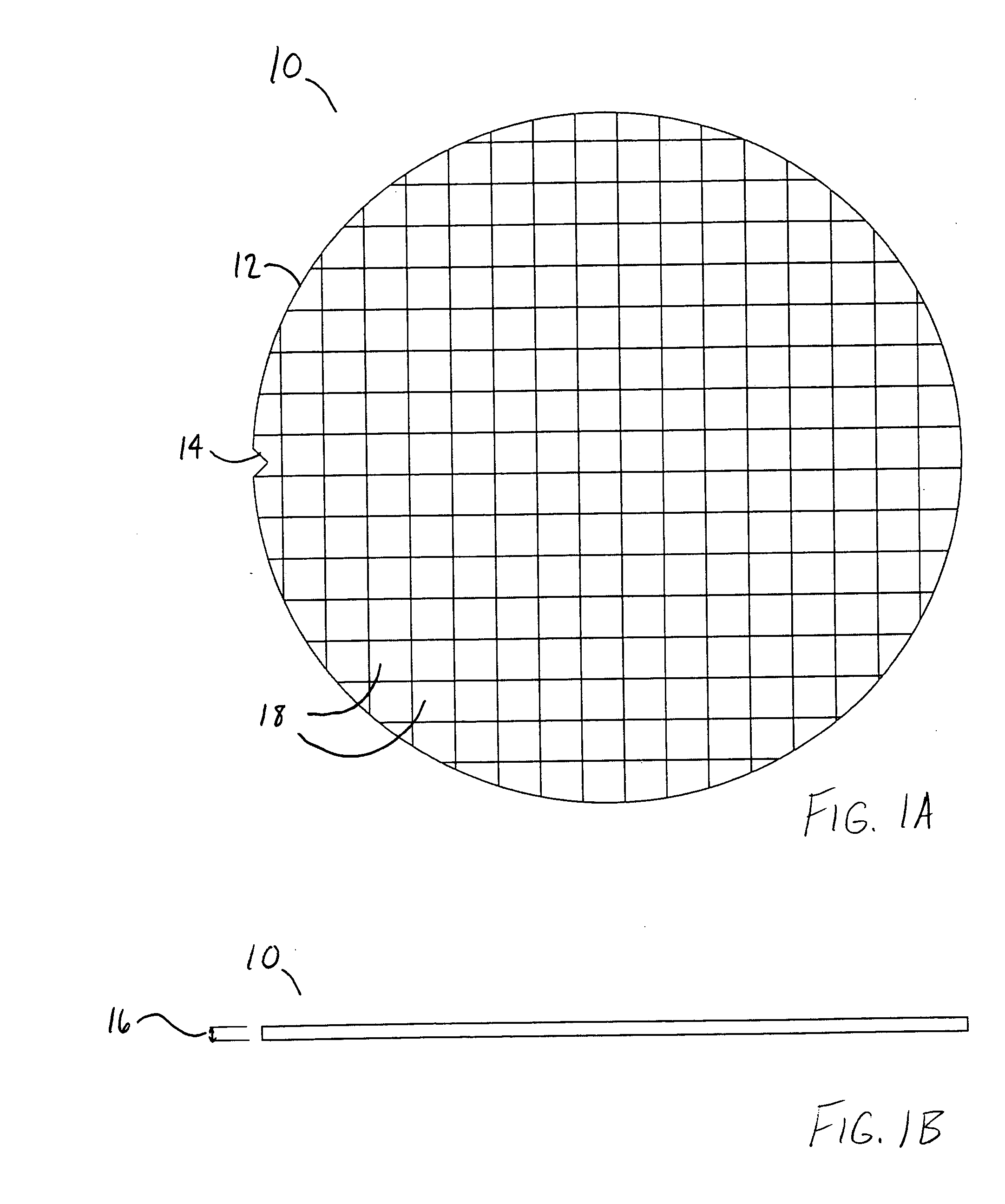
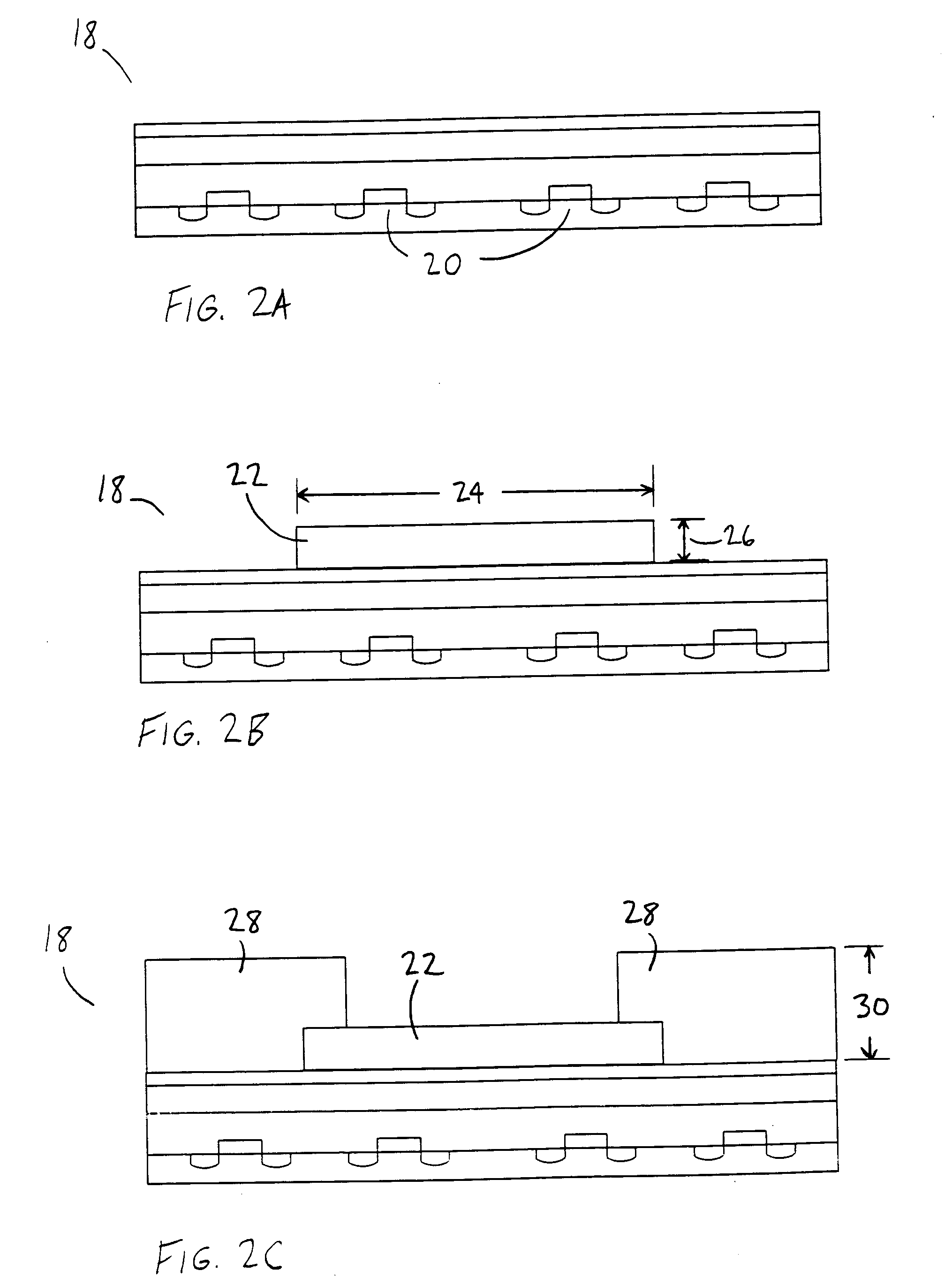
[0029]FIG. 1A to FIG. 7 illustrate electronic assemblies according to embodiments of the present invention. According to one aspect of the present invention, an electronic assembly includes a microelectronic die having an integrated circuit formed therein. Carbon nanotubes are grown on the microelectronic die and are electrically connected to the integrated circuit. The carbon nanotubes form a plurality of contact formations to connect the die, and the integrated circuit therein, to a package substrate. The package substrate may then be attached to a printed circuit board and installed in a computing system. According to another aspect of the present invention, a first conductive layer is formed on a semiconductor substrate having a plurality of transistors formed thereon. Then a second conductive layer is formed on the first conductive layer. A hole is created at least partially through both the first and second conductive layers. Carbon nanotubes are grown within the hole to elect...


PUM


Abstract

According to one aspect of the invention, an electronic assembly is provided. The electronic assembly includes a microelectronic die having an integrated circuit formed therein. Carbon nanotubes are grown on the microelectronic die and are electrically connected to the integrated circuit. The carbon nanotubes form a plurality of contact formations to connect the die, and the integrated circuit therein, to a package substrate. The package substrate may then be attached to a printed circuit board and installed in a computing system. According to another aspect of the present invention, a first conductive layer is formed on a semiconductor substrate having a plurality of transistors formed thereon. Then a second conductive layer is formed on the first conductive layer. A hole is created at least partially through both the first and second conductive layers. Carbon nanotubes are grown within the hole to electrically interconnect the two conductive layers.

Description

BACKGROUND OF THE INVENTION [0001] 1). Field of the Invention [0002] Embodiments of this invention relate to an electronic assembly, and more particularly, how electrical connections are made between various components of the electronic assembly. [0003] 2). Discussion of Related Art [0004] Integrated circuits are formed on semiconductor wafers. The wafers are then sawed (or “singulated” or “diced”) into microelectronic dice, also known as semiconductor chips, with each chip carrying a respective integrated circuit. Each semiconductor chip is then mounted to a package, or carrier, substrate. Often the packages are then mounted to a motherboard, which may then be installed into a computing system. [0005] The package substrates provide structural integrity to the semiconductor chips and are used to connect the integrated circuits electrically to the motherboard. On the side of the of the package substrate connected to the motherboard there are Ball Grid Array (BGA) solder ball contact ...

Claims


Application Information

Patent Timeline
Patent Type & Authority Applications(United States)
IPC IPC(8): H01L21/60H01L23/485H01L23/532H01L29/15
CPCB82Y10/00H01L2224/1147H01L24/11H01L2221/1094H01L2224/13099H01L2924/01013H01L2924/01027H01L2924/01029H01L2924/01074H01L2924/01078H01L2924/01079H01L2924/14H01L24/13H01L2924/01006H01L2924/01033H01L2924/01045H01L2924/014H01L23/53276H01L2924/0001H01L2224/131H01L2924/00015H01L2924/12042H01L2224/05022H01L2224/05001H01L2224/05572H01L2224/05147H01L2224/05655H01L24/03H01L24/05H01L2924/00H01L2924/00014
Inventor WANG, YONGQIAN
Owner INTEL CORP
Why Eureka
Try Eureka