Light emitting display and fabrication method thereof

a technology fabrication method, which is applied in the direction of electroluminescent light sources, static indicating devices, instruments, etc., can solve the problems of non-uniform nature, large weight of crt display, disadvantages of light emitting display, etc., and achieve uniform picture quality

Inactive Publication Date: 2005-12-29
SAMSUNG MOBILE DISPLAY CO LTD
View PDF11 Cites 8 Cited by
  • Summary
  • Abstract
  • Description
  • Claims
  • Application Information

AI Technical Summary

Benefits of technology

[0010] Accordingly, it is an object of the present invention to provide a light emitting display and a fabrication method thereof, in which a stripe pattern due to non-uniform characteristics of a driving transistor is prevented, thereby providing uniform picture quality.

Problems solved by technology

Recently, various flat panel displays have been developed, which substitute for a cathode ray tube (CRT) display because the CRT display is relatively heavy and bulky.
However, such a light emitting display also has disadvantages.
For example, such a light emitting display typically has pixel circuits which employ driving thin film transistors (TFTs) which have characteristics which are non-uniform in nature.
In addition, light emitting displays are fabricated by utilization of a laser crystallization process which has certain advantages, but which is also burdened by a disadvantage in that energy deviation in a laser beam used in laser scanning operations causes variation in certain characteristics of a poly silicon formed as a result.

Method used


Image

  • Light emitting display and fabrication method thereof
  • Light emitting display and fabrication method thereof
  • Light emitting display and fabrication method thereof

Examples


first embodiment

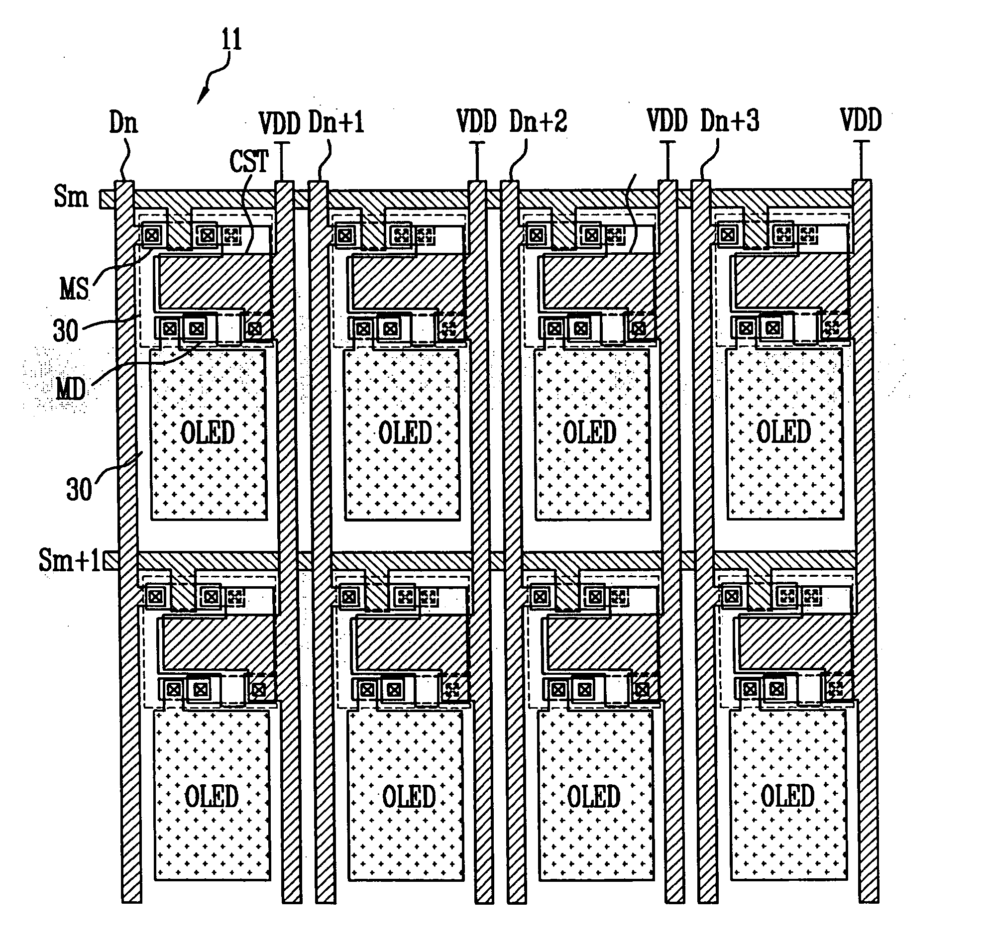
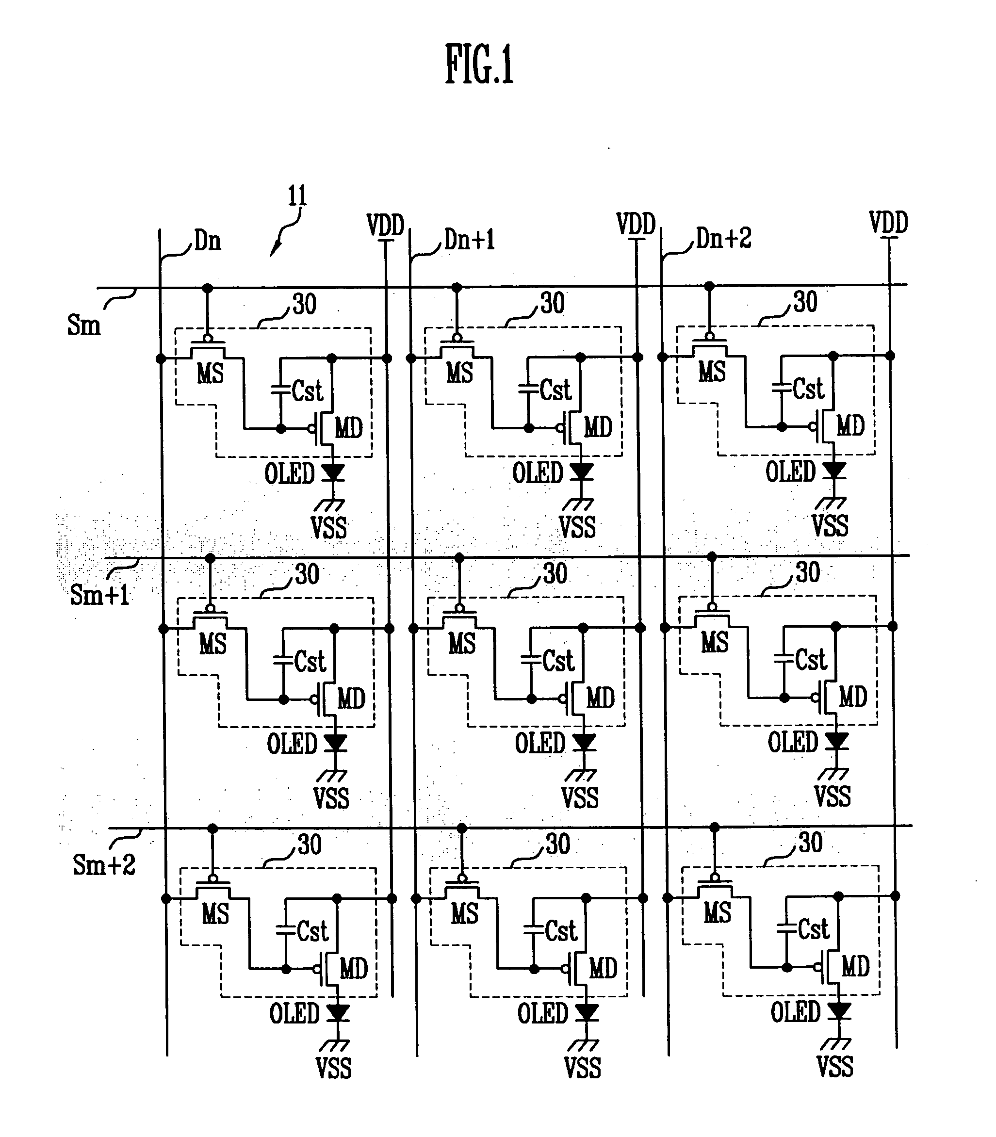
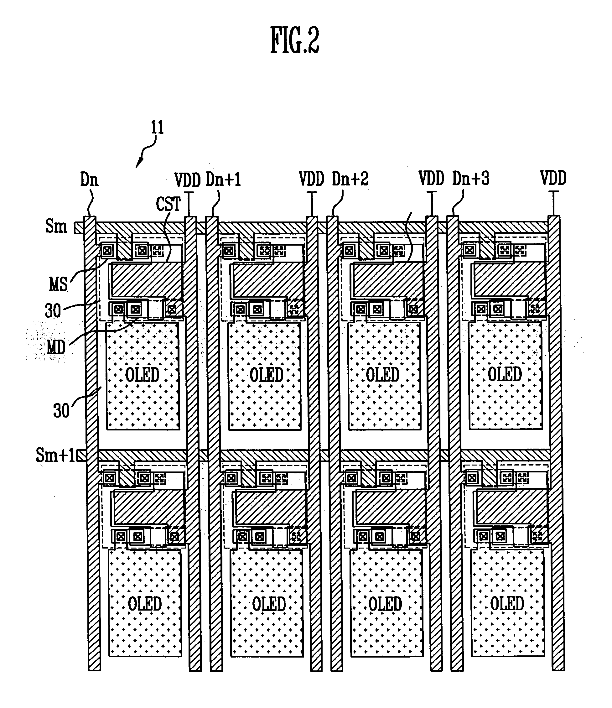
[0057] Referring to FIGS. 5 and 6, a light emitting display according to the present invention comprises a plurality of pixels 111 placed adjacent to regions where data lines D and scan lines S cross each other. Each pixel 111 comprises a pixel circuit 130 including an organic light emitting device OLED, and a driving thin film transistor (TFT) MD for supplying, to the organic light emitting device OLED, current corresponding to a data signal of the data line D. Furthermore, the positions of the driving TFTs MD are alternately varied in the a horizontal direction.

[0058] In each pixel 111, the pixel circuit 130 controls the organic light emitting device OLED to emit light. The scan line S is formed horizontally, and the data line D and a first power line VDD are formed vertically. Each pixel 111 receives a data signal from the data line D when a selection signal is applied to the scan line S, and emits light corresponding to the received data signal.

[0059] Each pixel 111 comprises: ...

second embodiment

[0086] As described above, in the light emitting display according to the present invention, the driving TFTs MD formed in the respective pixel circuits 130 are disposed in zigzag fashion with respect to the vertical direction, thereby compensating for the non-uniform characteristics, such as the threshold voltage, the mobility, etc., of the driving TFTs MD due to the laser crystallization process wherein amorphous silicon is crystallized into poly silicon. Therefore, the picture quality of the light emitting display is enhanced.

[0087] In more detail, in the light emitting display according to the second embodiment of the present invention, the excimer laser is applied differently to the respective semiconductor layers 104 of the adjacent driving TFTs MD with respect to the vertical direction, leaving a time lag. Furthermore, the excimer laser is applied differently to the respective semiconductor layers 104 of the adjacent driving TFTs MD with respect to the vertical direction, lea...


PUM


Abstract

In a light emitting display and a fabrication method thereof, a stripe pattern displayed due to characteristic differences of a driving transistor is prevented, thereby enhancing picture quality. The light emitting display comprises: a plurality of light emitting devices formed adjacent to a region where data and scan lines cross each other; and a plurality of pixel circuits, each including a driving transistor for supplying current corresponding to a data signal to a respective one of the light emitting devices. The positions of the driving transistors are different from each other with respect to at least one of horizontal and vertical directions. With this configuration, a stripe pattern is prevented from appearing perpendicular to a scanning direction of a line beam emitted from an excimer laser during the fabrication method.

Description

CLAIM OF PRIORITY [0001] This application makes reference to, incorporates the same herein, and claims all benefits accruing under 35 U.S.C. §119 from an application for LIGHTEMITTING DISPLAY AND FABRICATION METHOD THEREOF earlier filed in the Korean Intellectual Property Office on Jun. 25, 2004 and there duly assigned Serial No. 2004-48316. BACKGROUND OF THE INVENTION [0002] 1. Technical Field [0003] The present invention relates to a light emitting display and, more particularly, to a light emitting display and a fabrication method thereof, in which a stripe pattern displayed due to the characteristic difference of a driving transistor is prevented, thereby enhancing picture quality. [0004] 2. Related Art [0005] Recently, various flat panel displays have been developed, which substitute for a cathode ray tube (CRT) display because the CRT display is relatively heavy and bulky. Flat panel displays include a liquid crystal display (LCD), a field emission display (FED), a plasma disp...

Claims


Application Information

Patent Timeline
Patent Type & Authority Applications(United States)
IPC IPC(8): H01L21/00H01L21/77H05B33/00H01L27/12H01L27/32H01L29/18H05B33/26
CPCG09G2320/0233H01L27/1285H01L27/3262H01L27/3244H01L27/1296H10K59/1213H10K59/12H05B33/00H05B33/26
Inventor CHOI, WOONG-SIK
Owner SAMSUNG MOBILE DISPLAY CO LTD
Why Eureka
Try Eureka