
Distributed amplifier

a technology of distributed amplifiers and amplifiers, which is applied in the direction of amplifiers with coupling networks, amplifiers with semiconductor devices/discharge tubes, etc., can solve the problems of complicated wiring process, difficult miniaturization of circuits, and subject of distributed amplifiers, etc., to achieve simple structure and permit miniaturization

Active Publication Date: 2005-12-29
NEOPHOTONICS CORP
View PDF1 Cites 4 Cited by
  • Summary
  • Abstract
  • Description
  • Claims
  • Application Information

AI Technical Summary

Benefits of technology

[0018] An object of the present invention is to provide a distributed amplifier with a simple structure that permits miniaturization.
[0020] According to the present invention, the signal line and ground faces of the coplanar line, the signal line of the microstrip line, and the amplification transistors are formed on the upper face of the dielectric substrate. Therefore, all of the respective electrodes of the transistors can be connected to the signal lines and ground faces, and so forth, on the upper face of the dielectric substrate. Accordingly, viaholes need not be provided in the dielectric substrate in order to connect the transistors. As a result, a distributed amplifier with a simple structure that permits circuit miniaturization is obtained, and so forth.

Problems solved by technology

However, the distributed amplifier is subject to the following problems.
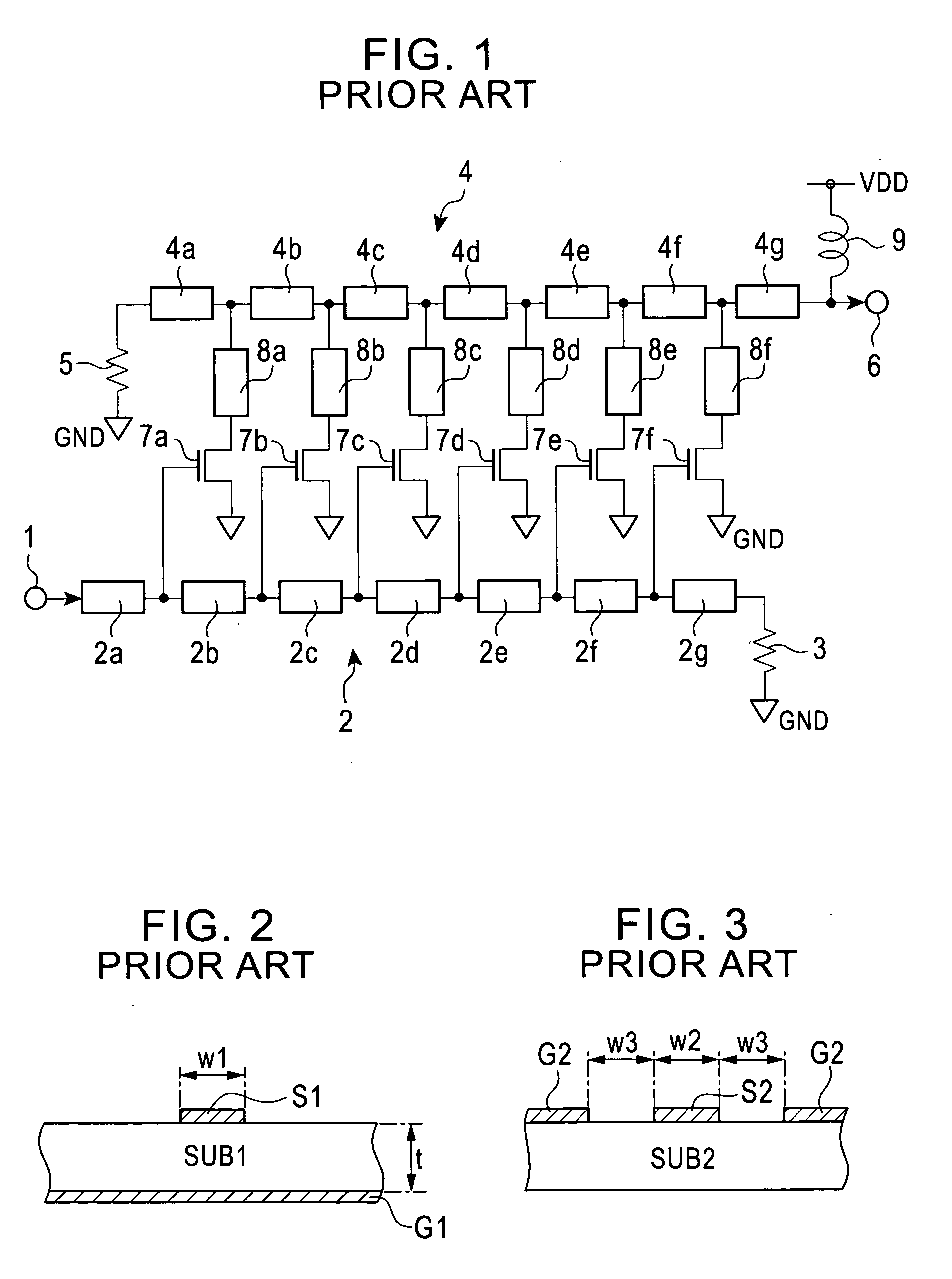
Therefore, viaholes must be provided in the dielectric substrate in order to reach ground via the shortest route as per the source electrodes of the transistors 7a to 9f in FIG. 1, which makes the wiring process complicated.
Therefore, miniaturization of the circuit is problematic.

Method used


Image

  • Distributed amplifier
  • Distributed amplifier
  • Distributed amplifier

Examples


Embodiment Construction

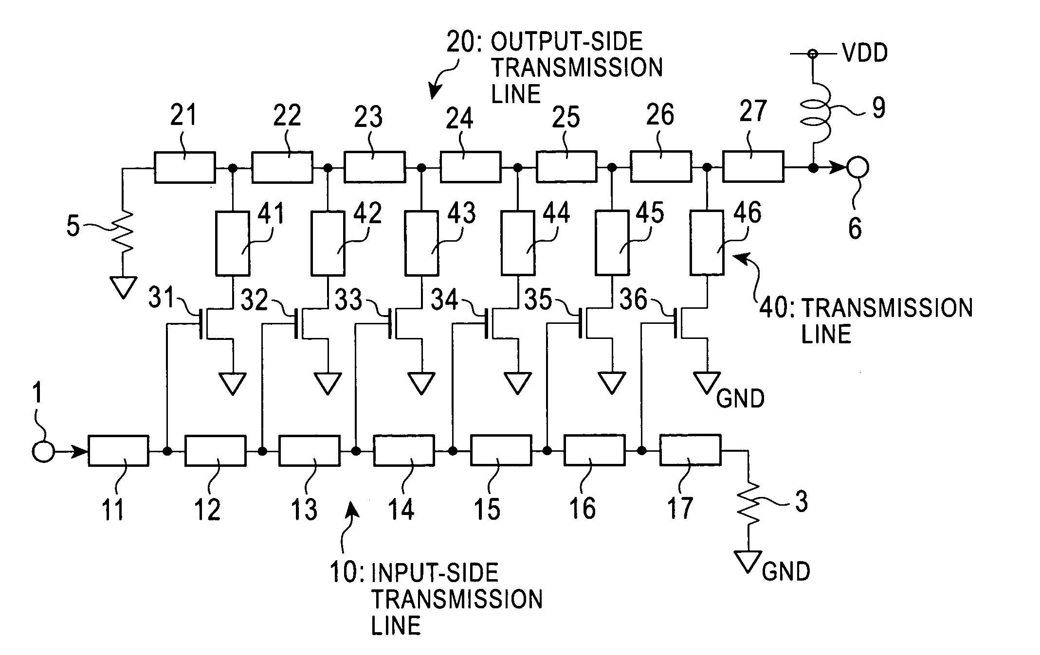
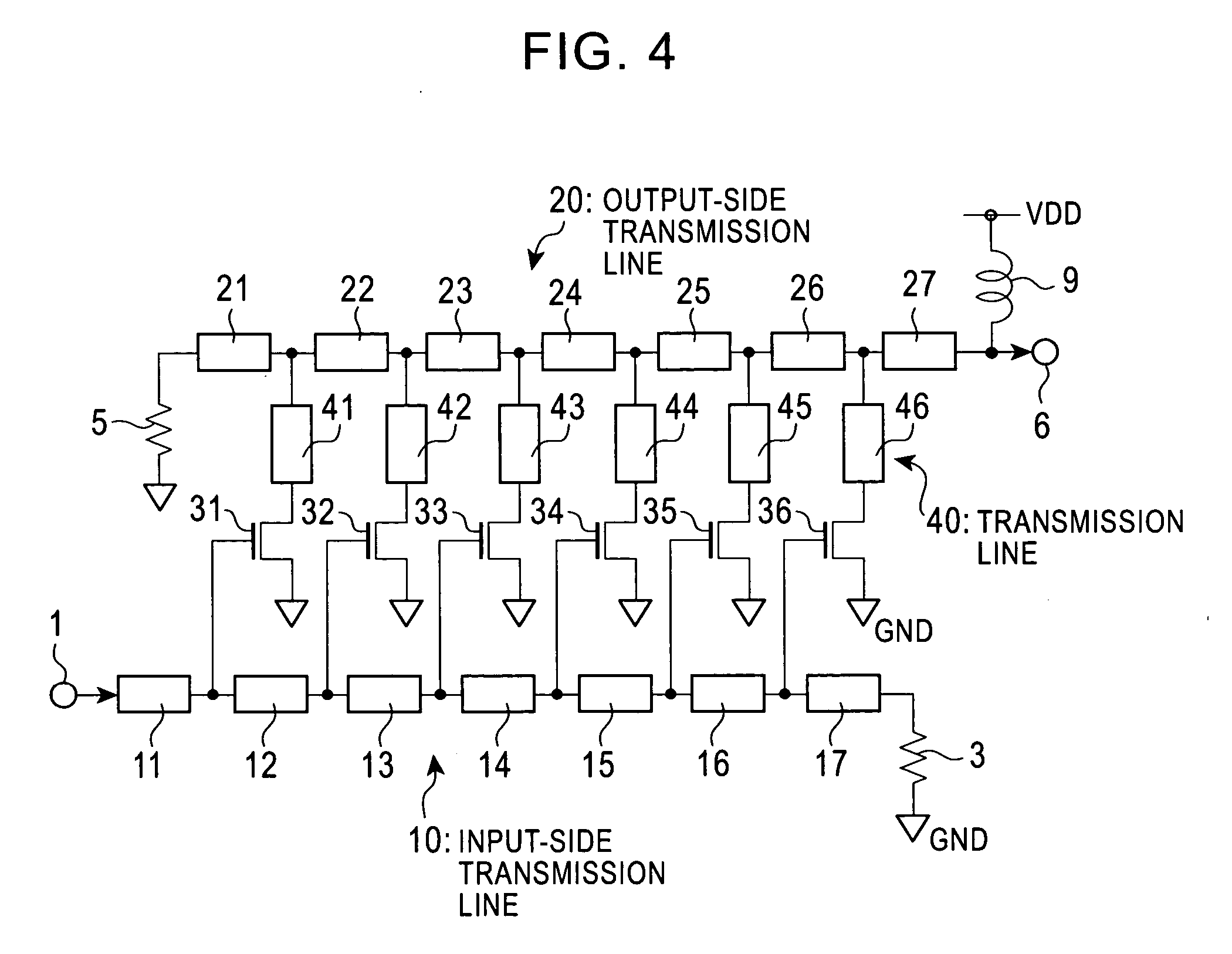
[0029]FIG. 4 is a constitutional view of the distributed amplifier illustrating the embodiment of the present invention. FIGS. 5 and 6 show the structure of the distributed amplifier in FIG. 4, where FIG. 5 is a planar view thereof and FIG. 6 is a partial cross-sectional view thereof along the line VI-VI in FIG. 5.

[0030] As the circuit constitution in FIG. 4 shows, the distributed amplifier comprises an input-side transmission line 10 that is connected to an input terminal 1 to which broad-range input signals are supplied and that constitutes an input-side filter. As shown in FIG. 6, the input-side transmission line 10 is a coplanar line that is constituted by the signal line S2 and ground faces G2 that are formed on the surface of the dielectric substrate SUB. In addition, the ground face G1 is provided over the whole of the rear face of the dielectric substrate SUB.

[0031] The input-side transmission line 10 serially connects seven line elements 11, 12, . . . , 17 such that the l...


PUM


Abstract

A distributed amplifier with a simple structure that permits miniaturization of circuit in which the input-side transmission line of the distributed amplifier is constituted by a coplanar line having a signal line and a ground face formed on the upper face of a dielectric substrate and the output-side transmission line of the distributed amplifier is constituted by a microstrip line having a signal line formed on the upper face of the dielectric substrate and a ground face formed on the lower face of the dielectric substrate. In addition, a plurality of amplification transistors is formed on the upper face of the dielectric substrate and each of the electrodes is connected to the signal line or the ground face that is formed on the upper face of the dielectric substrate. Because a large transistor-drive current does not flow to the input-side transmission line, the signal line can be made narrow and there is no increase in the required surface area even in the case of a coplanar line. Further, because the ground face of the coplanar line can be formed on the upper face of the dielectric substrate, the source electrodes or similar of the transistors can be grounded easily with a simple structure.

Description

BACKGROUND OF THE INVENTION [0001] 1. Field of the Invention [0002] The present invention relates to a distributed amplifier having a broadband characteristic that is employed in an optical communication system, for example. [0003] 2. Description of the Related Art [0004] The prior art includes Japanese Patent Kokai No. H7-183428 (Patent Document 1) and Japanese Patent Kokai No. 2003-152476 (Patent Document 2). [0005]FIG. 1 is a constitutional view of a conventional distributed amplifier. [0006] As per the circuit constitution shown in FIG. 1, this distributed amplifier comprises an input-side transmission line 2 connected to an input terminal 1 that is supplied with input signals over a wide range. The input-side transmission line 2 serially connects seven line elements 2a, 2b, . . . , 2g, for example. The leading terminal of line element 2a is connected to input terminal 1 and the end terminal of line element 2g is connected to the ground potential GND via a terminator 3. [0007] T...

Claims


Application Information

Patent Timeline
Patent Type & Authority Applications(United States)
IPC IPC(8): H01L27/02H03F3/60
CPCH03F3/605H01L27/0207H03F3/60
Inventor KOSUGI, MAKOTONISHINO, AKIRAOGAWA, YASUNORI
Owner NEOPHOTONICS CORP
Learn More