

Radiation hardened bipolar junction transistor
a bipolar junction transistor, radiation hardening technology, applied in the direction of semiconductor/solid-state device details, semiconductor devices, electrical devices, etc., can solve the problems of junction leakage and gain degradation, low mobility, and prone to oxide trapped in the oxide, so as to improve the sensitivity of bjts, improve the sensitivity, and reduce the effect of oxidation
- Summary
- Abstract
- Description
- Claims
- Application Information
AI Technical Summary
Benefits of technology
Problems solved by technology
Method used
Image

Examples
Embodiment Construction
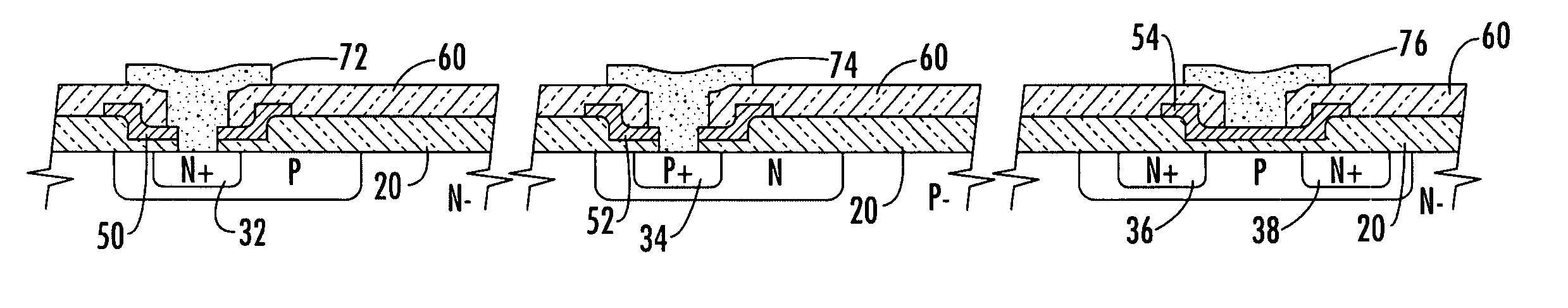
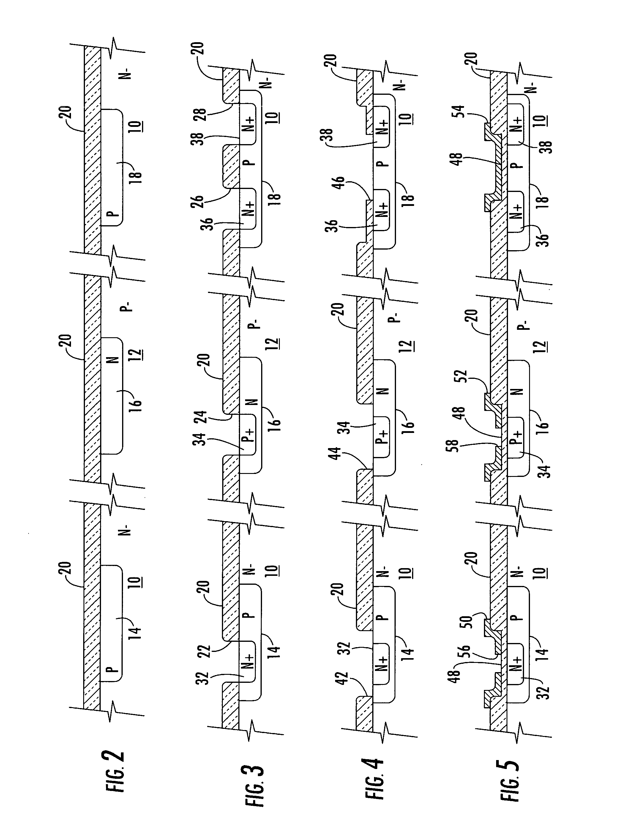
[0019] In prior art devices, the thick, unhardened oxide or dielectric over the emitter-base junctions of the BJT traps positive charge efficiently. If this dielectric could be made thinner, the volume available for charge trapping would be reduced, and the device hardness would improve. The thin dielectric may also be hardened by several well-known methods, which would reduce charge trapping further. Additionally, a field plate covering the junction would positively control the potential at the silicon surface. As most BiMOS processes have a thin gate oxide and a gate polycrystalline layer, the revised BJT structures can be built readily and without any additional masking levels. An example of a conventional, non-hardened thin oxide is that used for on-chip MOS capacitors.
[0020] This structure results in a field plate over the emitter-base junction, with thin oxide under the field plate. The thin oxide may be hardened or non-hardened, depending on the process being used. The field...
PUM
 Abstract
Description
Claims
Application Information