[0008] The present invention is made in consideration for the foregoing problems. A method for manufacturing a
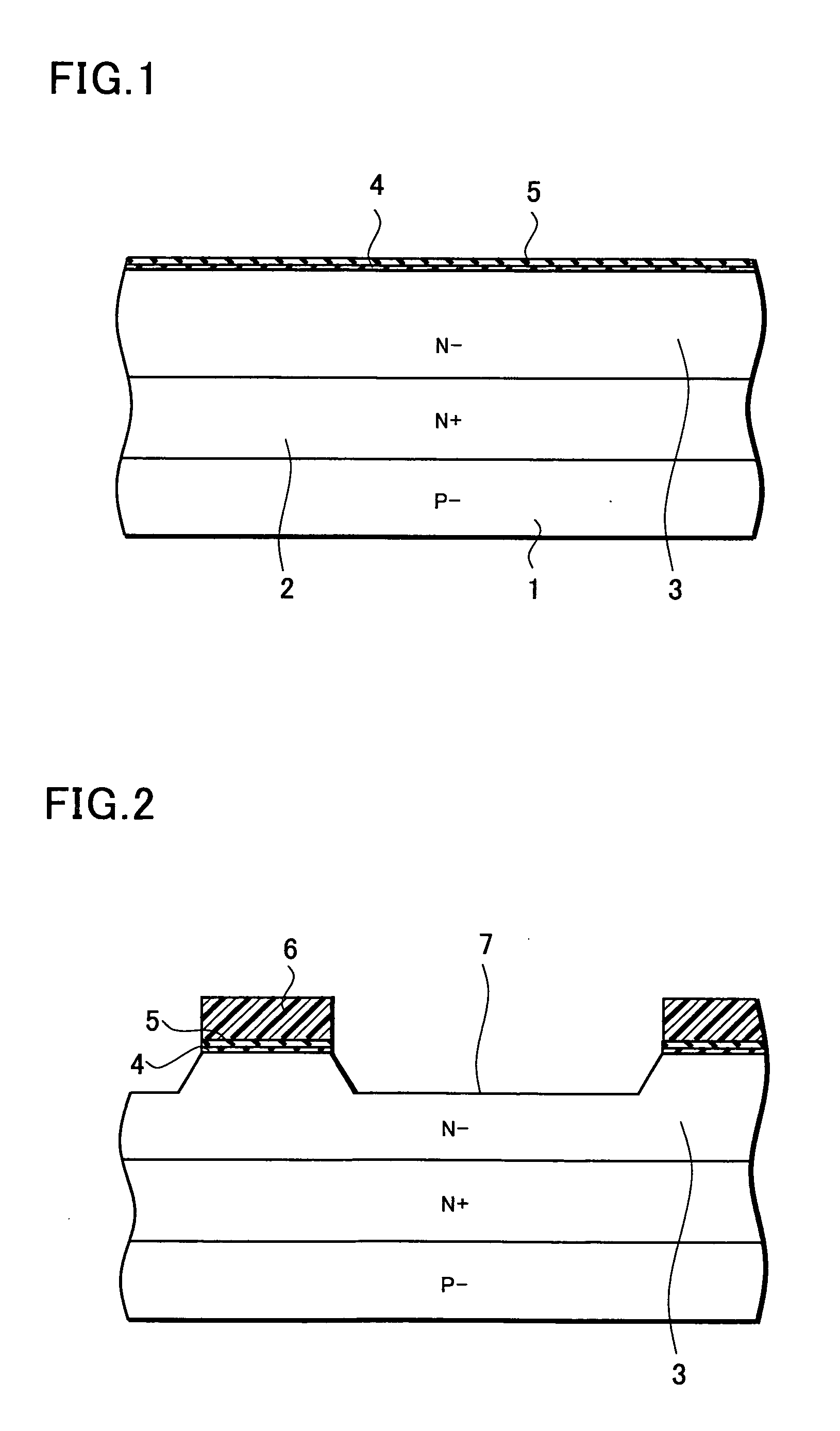
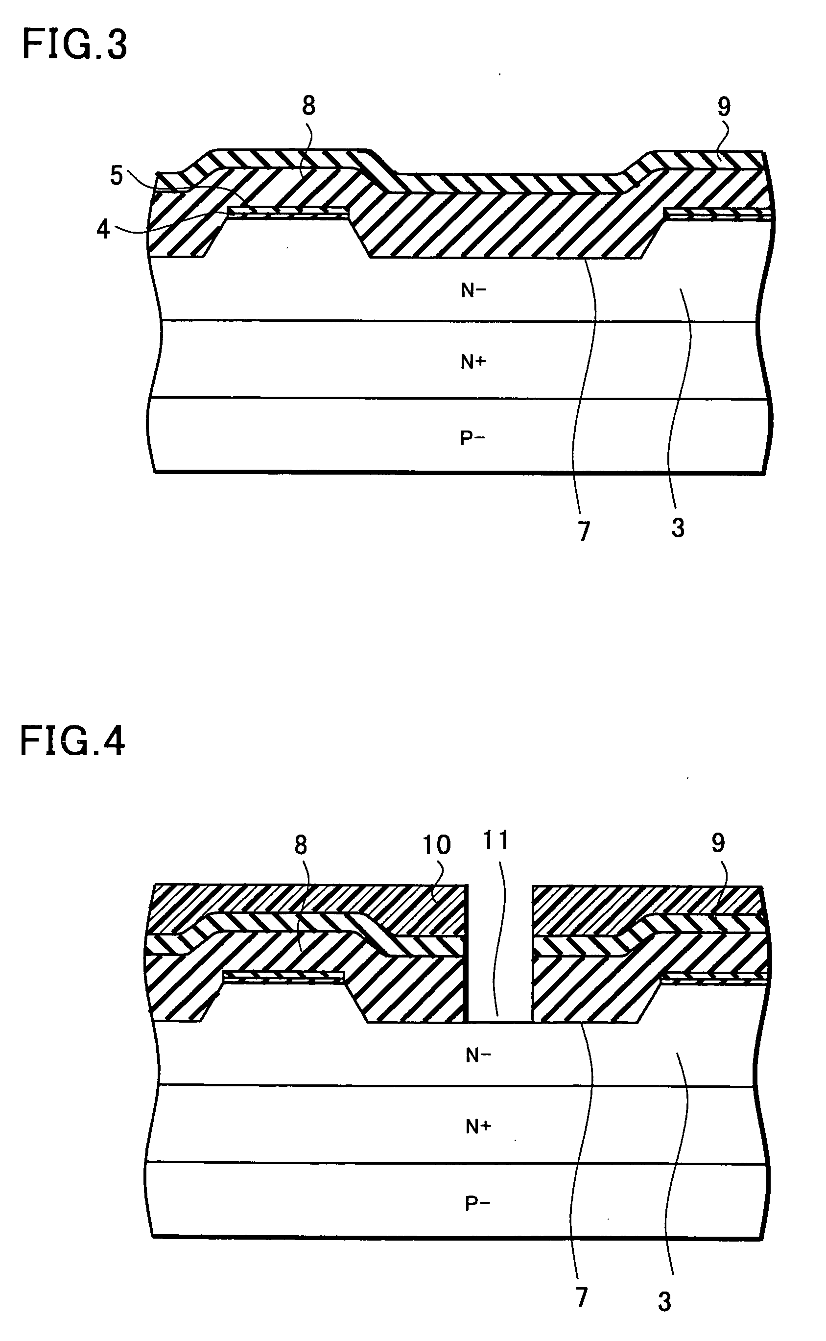
semiconductor device of the present invention includes the steps of forming a first insulating film on a surface of a semiconductor layer, the first insulating film having an opening provided in a desired region, and forming a groove in the semiconductor layer through the opening; forming a second insulating film so as to fill up the groove, and forming a trench from a surface of the second insulating film; forming a third insulating film on the second insulating film, forming a
polycrystalline silicon film on the third insulating film, and filling the trench with the third insulating film and the
polycrystalline silicon film;
polishing the second insulating film, the third insulating film and the
polycrystalline silicon film by use of the first insulating film as a stopper film; and forming an insulating spacer in a concave part formed by partially removing the third insulating film when the first insulating film is removed by
etching. Therefore, the method of the present invention includes the step of forming the insulating spacer for the concave part in an upper part of the third insulating film, which is formed when the first insulating film is removed. Thus, it is possible to prevent a material such as the polycrystalline
silicon film used in the other steps from remaining in the concave part. Moreover, by filling the concave part with the insulating spacer, a flat upper surface of an isolation region can be realized, and a passive element such as a capacity element can be formed on the upper surface of the isolation region. Moreover, it is possible to prevent disconnection of a wiring layer on the upper surface of the isolation region.
[0009] Moreover, in the method for manufacturing a
semiconductor device of the present invention, the second insulating film is formed by depositing a HTO (high temperature
oxide) film on an NSG (non-doped-
silicate glass) film by use of a low pressure CVD method, the NSG film being deposited by use of a
high density plasma CVD (HDP CVD) method. Therefore, in the present invention, the NSG film deposited by use of the
high density plasma CVD method has a good filling property, and the groove in the semiconductor layer can be filled up with the NSG film. Moreover, the HTO film deposited by use of the low pressure CVD method has a good step covering property, and can be used as a
hard mask in formation of the trench.
[0010] In the present invention, after the HTO film is deposited in the trench which forms the isolation region, the polycrystalline silicon film is deposited on the HTO film to fill up the trench. Accordingly, an amount of the polycrystalline silicon film deposited is reduced, and an amount of the films polished by use of the CMP method is also reduced. Thus, manufacturing costs can be suppressed.
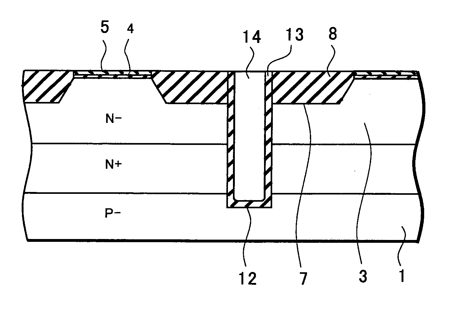
[0011] Moreover, in the present invention, when a
thermal oxide film used for the STI method is removed, a part of the HTO film in the trench is removed, and the concave part is formed in the isolation region. However, in the subsequent step, the concave part is filled up with an insulating spacer formed of a TEOS (
tetra ethyl ortho
silicate) film. Thus, flatness in the isolation region can be realized. Consequently, it is possible to reduce a residue of a polysilicon film and the like, which remains in the concave part in the other steps. Moreover, short-circuiting caused by the residue, which is removed from the concave part and reaches an element formation region, is prevented. Thus, yield can be improved. Meanwhile, by realizing the flat upper surface of the isolation region, the passive element such as the capacity element, for example, can be formed on the upper surface of the isolation region. Moreover, disconnection of the wiring layer formed on the upper surface of the isolation region can be prevented.

