Liquid precursors for the CVD deposition of amorphous carbon films

a carbon film and liquid precursor technology, applied in the direction of chemical vapor deposition coating, coating, metallic material coating process, etc., can solve the problems of difficulty in producing features with little or no surface defects or feature deformation, increase the likelihood of defects being formed on the substrate surface, and low k materials are often brittle and may deform under conventional polishing processes

Active Publication Date: 2005-12-29
APPLIED MATERIALS INC
View PDF77 Cites 662 Cited by
  • Summary
  • Abstract
  • Description
  • Claims
  • Application Information

AI Technical Summary

Benefits of technology

[0014] Aspects of the invention generally provide a method for depositing amorphous carbon materials. In one aspect, the invention provides a method for processing a substrate including positioning the substrate in a processing chamber, introducing a processing gas into the processing chamber, wherein the processing gas includes one or more hydrocarbon compounds or derivatives thereof, and hydrogen, generating a plasma of the processing gas by applying power from a dual-frequency RF source, and depositing an amorphous carbon layer on the substrate.
[0015] In another aspect of the invention, a method is provided for processing a substrate including forming a dielectric material layer on a surface of the substrate, depositing one or more amorphous carbon layers on the dielectric material layer by a process including introducing a processing gas includes one or more hydrocarbon compounds and hydrogen, generating a plasma of the processing gas by applying power from a dual-frequency RF source, etching the one or more amorphous carbon layers to form a patterned amorphous

Problems solved by technology

However, it has been difficult to produce features with little or no surface defects or feature deformation when low k materials have been used in damascene formation.
Low k dielectric materials are often porous and susceptible to being scratched and damaged during removal of conductive materials, thus increasing the likelihood of defects being formed on the substrate surface.
Further, low k materials are often brittle and may deform under conventional polishing processes.
Such thinner resist materials (less than about 6000 Å) can be insufficient to mask underlying material layers during a pattern transfer step using a chemical etchant.
However, in some applications for forming semiconductor structures, it is difficult to remove hardmask materials from the substrate surface and the remaining hardmask material may detrimentally affect semiconductor processing.
Further, conventional hardmask materials may not provide sufficient etch selectivity between the material being

Method used


Image

  • Liquid precursors for the CVD deposition of amorphous carbon films
  • Liquid precursors for the CVD deposition of amorphous carbon films
  • Liquid precursors for the CVD deposition of amorphous carbon films

Examples


Embodiment Construction

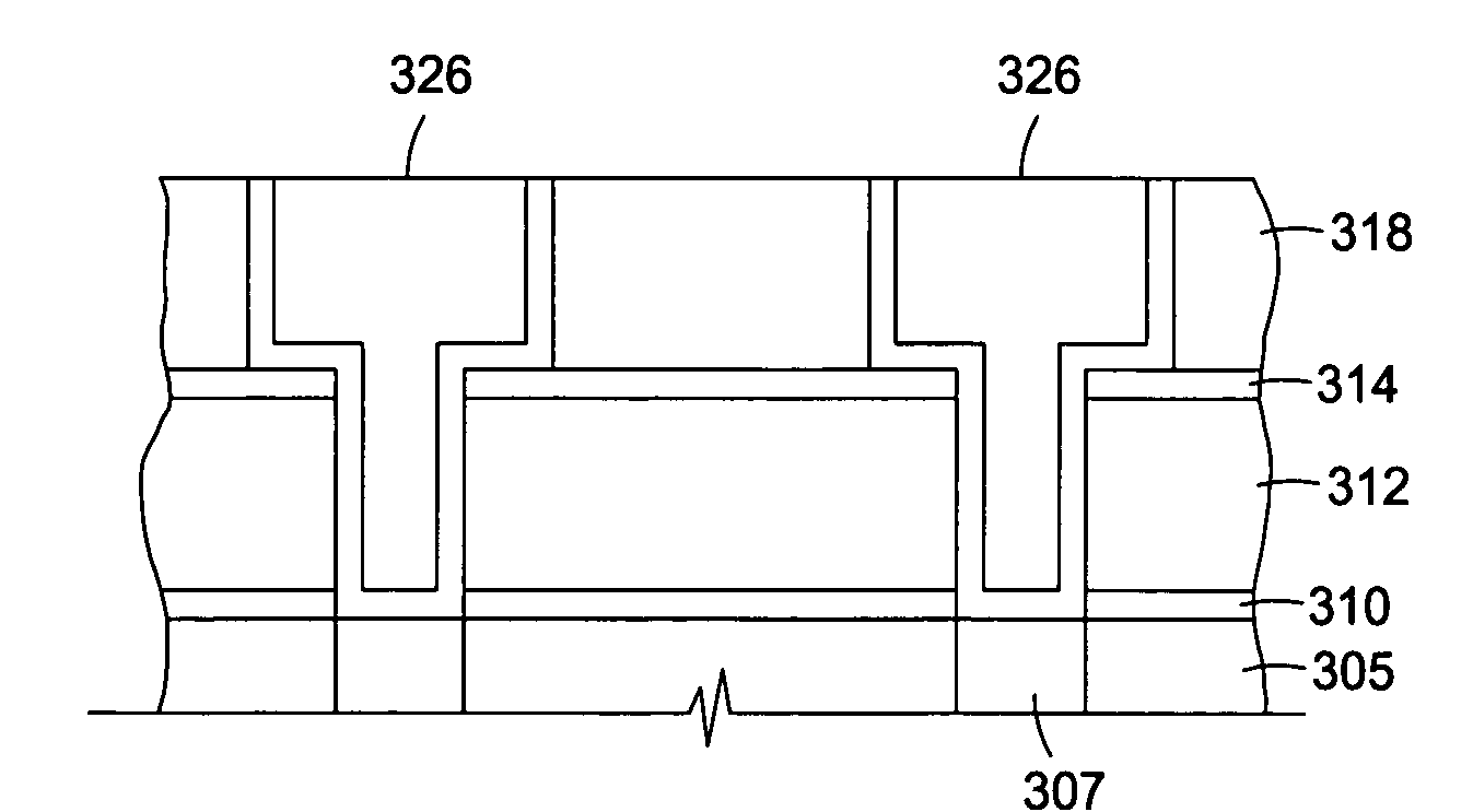
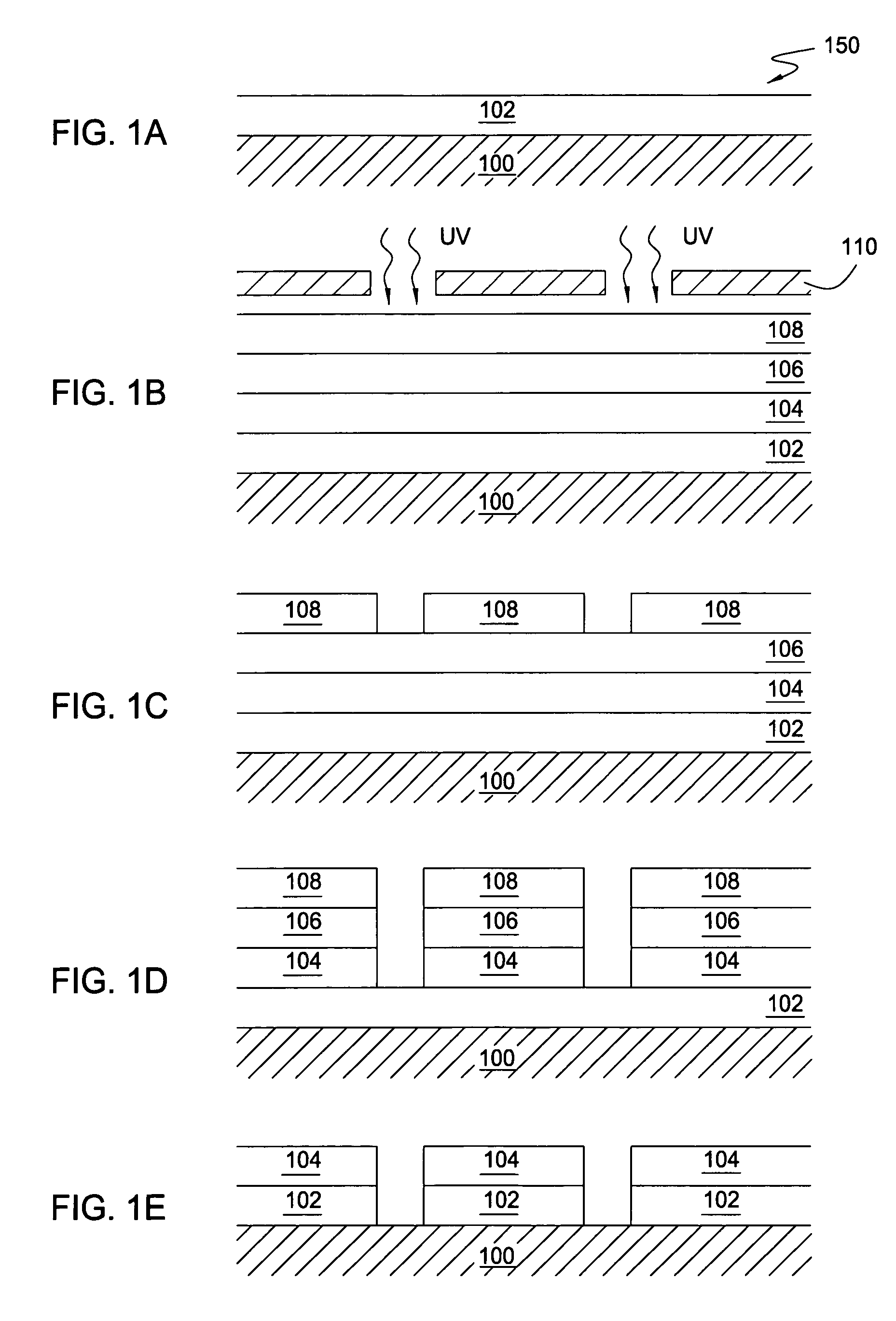
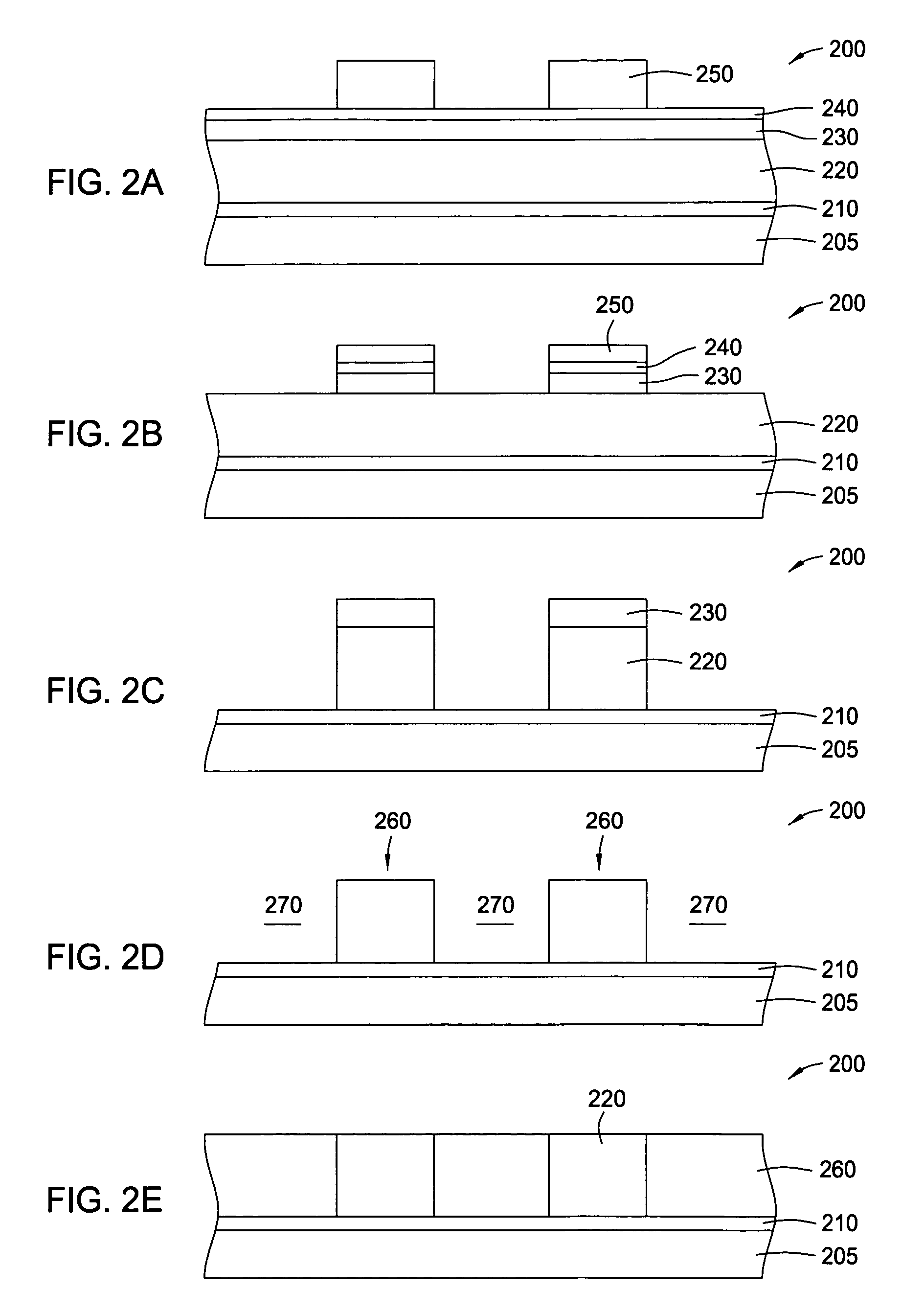
[0025] The words and phrases used herein should be given their ordinary and customary meaning in the art by one skilled in the art unless otherwise further defined. Aspects of the invention generally provide methods for depositing, processing, and removing amorphous carbon material. Amorphous carbon deposition rates and etch selectivity to dielectric materials, such as oxides, may be increased compared to amorphous carbon deposited by conventional amorphous carbon deposition processes by the use of dual frequency RF power sources and the inclusion of hydrogen as a diluent gas and argon as a carrier gas in amorphous carbon processing gases. Amorphous carbon deposition is further described in U.S. Pat. No. 6,573,030, issued on Jun. 3, 2003, entitled, “Method for Depositing an Amorphous Carbon Layer”, which is hereby incorporated by reference herein to the extent not inconsistent with the claimed aspects and description herein.

[0026] Examples of suitable systems include the CENTURA® s...


PUM

PropertyMeasurementUnit
Temperatureaaaaaaaaaa
Poweraaaaaaaaaa
Poweraaaaaaaaaa

Abstract

Methods are provided for depositing amorphous carbon materials. In one aspect, the invention provides a method for processing a substrate including positioning the substrate in a processing chamber, introducing a processing gas into the processing chamber, wherein the processing gas comprises a carrier gas, hydrogen, and one or more precursor compounds, generating a plasma of the processing gas by applying power from a dual-frequency RF source, and depositing an amorphous carbon layer on the substrate.

Description

CROSS-REFERENCE TO RELATED APPLICATIONS [0001] This application is a continuation-in-part of co-pending U.S. patent application Ser. No. 10 / 799,146, filed Mar. 12, 2004, and claims benefit of U.S. provisional patent application Ser. No. 60 / 550,386, filed Mar. 3, 2004, U.S. provisional patent application Ser. No. 60 / 565,639, filed Apr. 26, 2004, and U.S. provisional patent application Ser. No. 60 / 649,344, filed Feb. 2, 2005. Each of the aforementioned related patent applications is herein incorporated by reference.BACKGROUND OF THE INVENTION [0002] 1. Field of the Invention [0003] The invention relates to the fabrication of integrated circuits and to a process for depositing materials on a substrate and to the structures formed by the materials. [0004] 2. Description of the Related Art [0005] The fabrication of modern semiconductor devices requires the formation of metal and dielectric layers on a substrate by chemical reaction of gases, referred to as chemical vapor deposition, CVD....

Claims


Application Information

Patent Timeline
IPC IPC(8): C23C16/505H01L21/314H01L21/768
CPCC23C16/505H01L21/3146H01L21/76829H01L21/76802H01L21/7681H01L21/76801H01L21/02274H01L21/02115H01L21/02205H01L21/02126H01L21/0217H01L21/02167H01L21/31
Inventor SEAMONS, MARTIN JAYYEH, WENDY H.RATHI, SUDHA S.R.PADHI, DEENESHTANG, SUM-YEE BETTYKULKARNI, PRIYASIVARAMAKRISHNAN, VISWESWARENKIM, BOK HOENM'SAAD, HICHEMWANG, YUXIANG MAYKWAN, MICHAEL CHIU
Owner APPLIED MATERIALS INC
Why Eureka
Try Eureka