Laser-based method and system for processing targeted surface material and article produced thereby

a surface material and laser technology, applied in the field of laser marking and texturing, can solve the problems of continued shrinkage of die size, unsuitable for present and emerging requirements, and traditional wafer marking systems, and achieve the effect of reducing reflection of energy used and increasing surface roughness

Inactive Publication Date: 2006-01-05
ELECTRO SCI IND INC
View PDF99 Cites 129 Cited by
  • Summary
  • Abstract
  • Description
  • Claims
  • Application Information

AI Technical Summary

Benefits of technology

[0015] In carrying out the above objects and other objects of the present invention, a method for processing targeted surface material within a region of a workpiece while avoiding undesirable changes to adjacent non-targeted material is provided. The method includes generating a pulsed laser output including at least one pulse having a wavelength and a pulse width. The method further includes irradiating the targeted surface material of the workpiece with the pulsed laser output including the at least one pulse to texture the targeted surface material. The pulsed laser output has sufficient total fluence to initiate ablation within at least a portion of the targeted surface material and the pulse width is short enough such that the region and non-targeted material surrounding the region are substantially free of slag.
[0039] The step of irradiating may substantially increase surface roughness of the targeted surface material within at least a portion of the region.
[0064] The step of irradiating with the secondary laser output may trim an electrical or mechanical parameter of the textured surface material.
[0067] Further in carrying out the above objects and other objects of the present invention, a system for processing targeted surface material within a region of a workpiece while avoiding undesirable changes to adjacent non-targeted material is provided. The system includes a primary laser subsystem which includes a primary laser source for generating a pulsed laser output including at least one pulse having a wavelength and a pulse width. The system further includes a delivery subsystem for irradiating the targeted surface material of the workpiece with the pulsed laser output including the at least one pulse to texture the targeted surface material. The pulsed laser output has sufficient total fluence to initiate ablation within at least a portion of the targeted surface material. The pulse width is short enough such that the region and the non-targeted material surrounding the material are substantially free of slag.
[0103] Yet still further in carrying out the above objects and other objects of the present invention, an article of manufacture is provided. At least one surface material has discernible indicia formed thereon during at least one step of manufacturing the article. The indicia are formed by a method of selectively irradiating targeted surface material within a region of a workpiece with a pulsed laser output. The indicia are at least semi-permanent and useable during a subsequent step of manufacturing the article. The region and non-targeted material surrounding the region are substantially slag-free. Surface roughness is increased within at least a portion of the region during the at least one step of manufacturing, thereby reducing reflection of energy used for reading the indicia.

Problems solved by technology

One of the emerging challenges for die marking is the recent introduction of very thin wafers.
Another challenge is the continuing shrinking of die sizes.
Traditional wafer marking systems are not well suited to present and emerging requirements.

Method used


Image

  • Laser-based method and system for processing targeted surface material and article produced thereby
  • Laser-based method and system for processing targeted surface material and article produced thereby
  • Laser-based method and system for processing targeted surface material and article produced thereby

Examples


Embodiment Construction

[0133] For the purpose of the following description of various embodiments of the invention, the following non-limiting guidelines are used:

[0134]“Ultrafast laser” or “ultrashort laser” generally refers to a pulsed laser providing one or more pulses, each pulse having a duration below 1 ns, for instance 100 ps or less, or typically less than 10 ps;

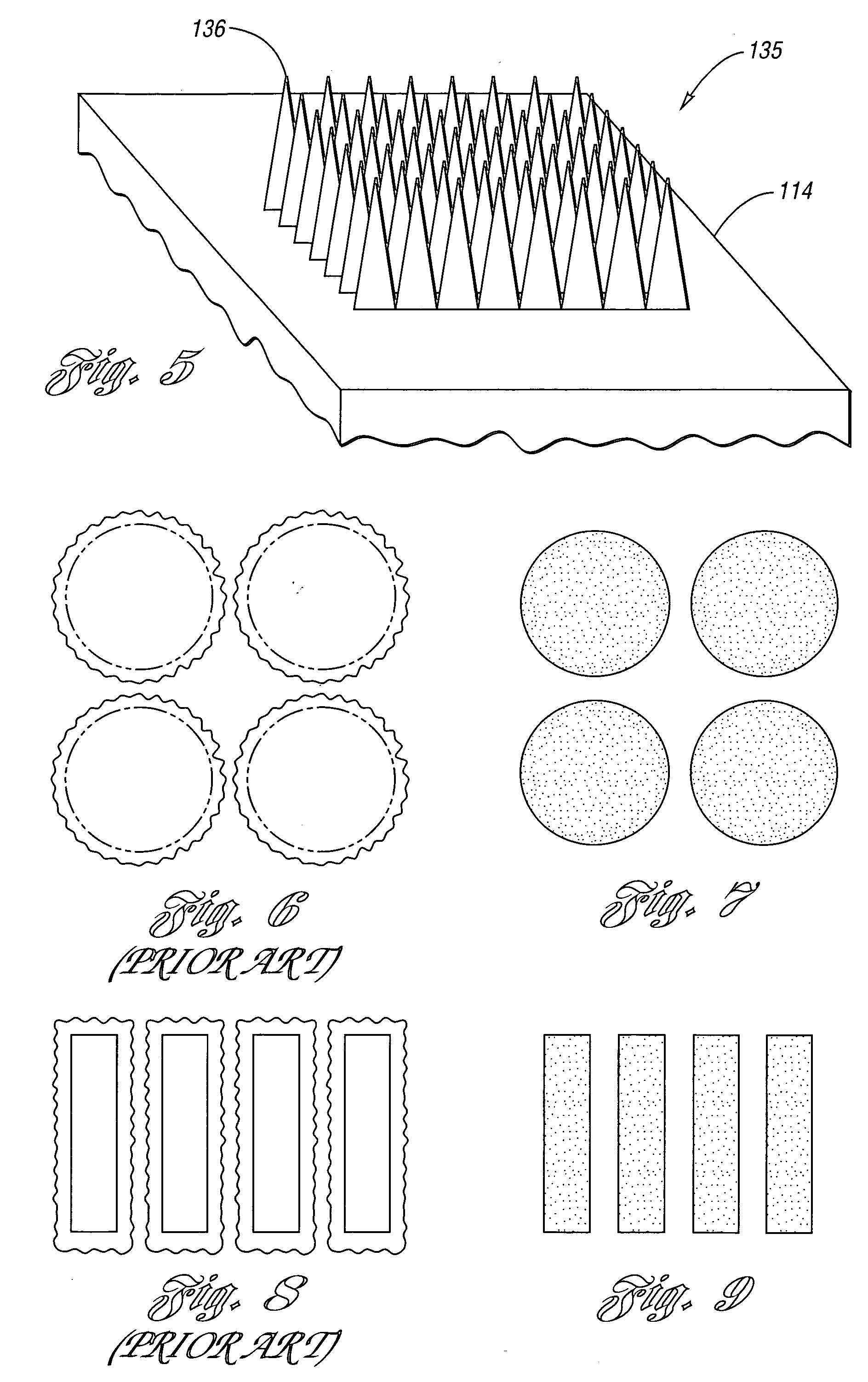
[0135]“Microtexture” generally refers to micron sized surface variations, but may also include surface variations of a finer scale, for instance 0.5 microns or 0.1 microns; and

[0136]“Nanotexture” generally refers to surface variations below one micron in size.

Overview

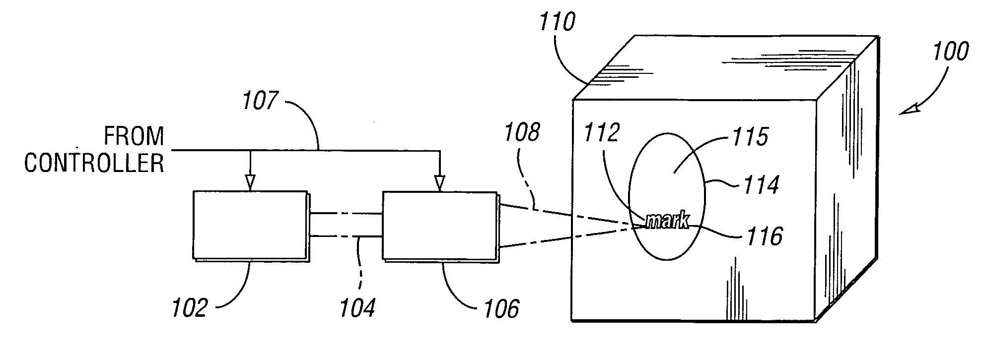
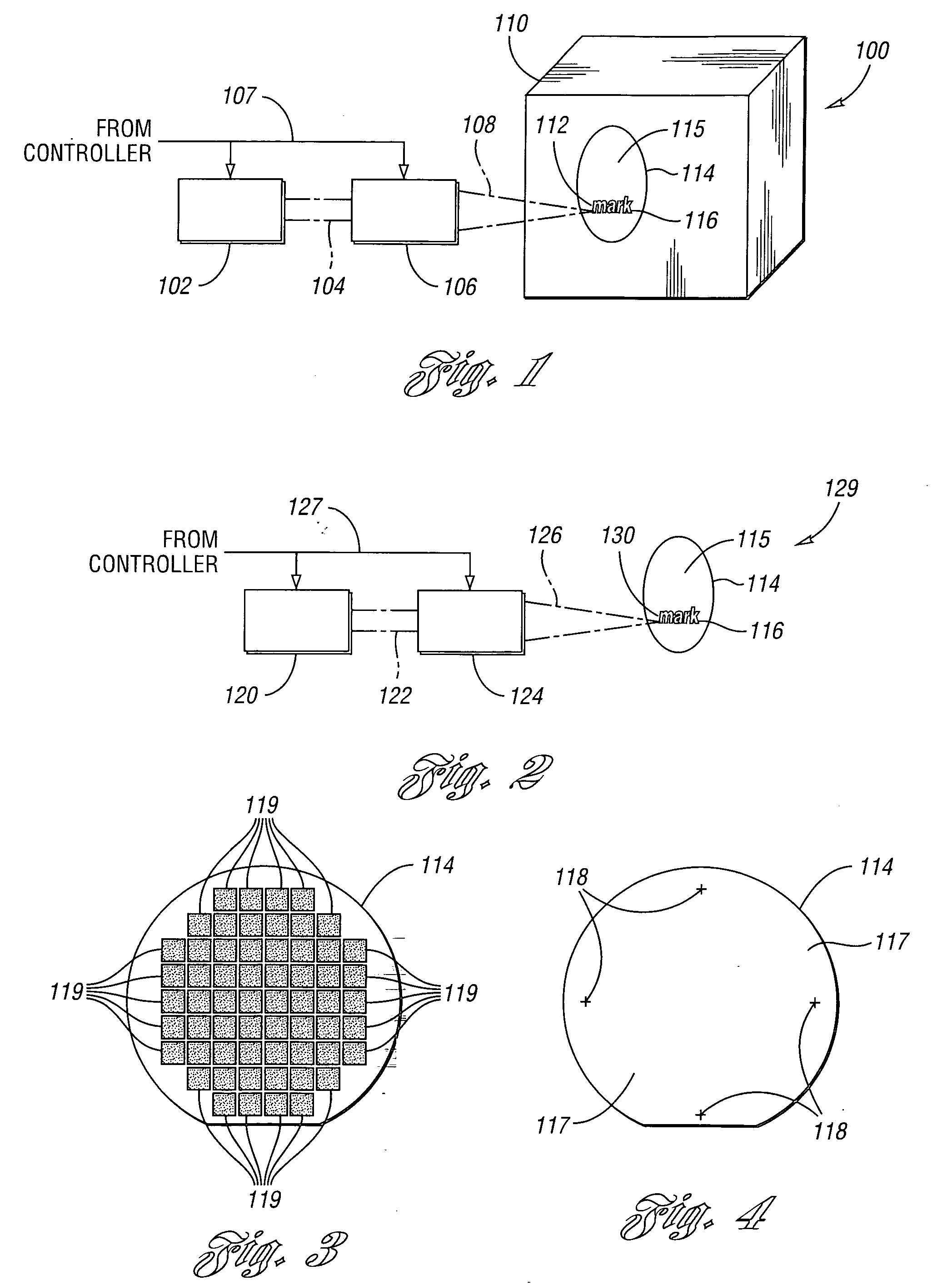
[0137] New laser marking technology has been developed to overcome limitations of present laser marking systems. Permanent and high contrast shallow marks (less than 1 micron) on the backside of wafers are achieved with little or no material removed by using this new laser technology. Viewing of these marks is strongly independent of the viewing angle, a significant adva...


PUM

PropertyMeasurementUnit
sizeaaaaaaaaaa
thicknessaaaaaaaaaa
thicknessaaaaaaaaaa

Abstract

A laser-based method and system for processing targeted surface material and article produced thereby are provided. The system processes the targeted surface material within a region of a workpiece while avoiding undesirable changes to adjacent non-targeted material. The system includes a primary laser subsystem including a primary laser source for generating a pulsed laser output including at least one pulse having a wavelength and a pulse width less than 1 ns. A delivery subsystem irradiates the targeted surface material of the workpiece with the pulsed laser output including the at least one pulse to texture the targeted surface material. The pulsed laser output has sufficient total fluence to initiate ablation within at least a portion of the targeted surface material and the pulse width is short enough such that the region and the non-targeted material surrounding the material are substantially free of slag.

Description

CROSS-REFERENCE TO RELATED APPLICATION [0001] This application claims the benefit of U.S. provisional application Ser. No. 60 / 584,268, filed Jun. 30, 2004.BACKGROUND OF THE INVENTION [0002] 1. Field of the Invention [0003] The present invention relates to laser marking and texturing, particularly forming at least semi-permanent or erasable indicia on one or more materials of a microelectronic device. The materials may include semiconductor substrates, thin films, metallization, and dielectric layers. One or more embodiments may also be applied for forming indicia on MEMs, optoelectronic devices, or biomedical microchips. Various embodiments are useable for various micromachining or microfabrication applications. [0004] 2. Background Art [0005] Prior to 1999, Silicon wafer marking was used for identification at wafer level. Initially driven by the Known Good Die, and more recently by traceability and component identification, laser marking on the backside of the wafer at the die leve...

Claims


Application Information

Patent Timeline
Patent Type & Authority Applications(United States)
IPC IPC(8): B23K26/36G01Q30/02G01Q60/00
CPCB23K26/0084B23K26/0635B23K26/0676B23K26/365H05K3/0026B41M5/24G06K1/126H05K1/0266B23K26/4075B23K26/40B33Y80/00B23K26/0624B23K26/361B23K26/355B23K2103/50H01L23/544H01L2223/54406H01L2223/54413H01L2223/54426H01L2223/54433H01L2223/54453
Inventor GU, BOEHRMANN, JONATHAN S.SVETKOFF, DONALD J.CAHILL, STEVEN P.SULLIVAN, KEVIN E.
Owner ELECTRO SCI IND INC
Why Eureka
Try Eureka