Digital delay locked loop capable of correcting duty cycle and its method

a technology of duty cycle and delay lock, which is applied in the direction of digital storage, oscillator generator, pulse technique, etc., can solve the problems of increasing the size increasing the power consumption of the semiconductor memory device, so as to reduce the length of the delay line and reduce the delay locking time

Active Publication Date: 2006-01-05
SK HYNIX INC
View PDF7 Cites 24 Cited by
  • Summary
  • Abstract
  • Description
  • Claims
  • Application Information

AI Technical Summary

Benefits of technology

[0027] It is, therefore, an object of the present invention to provide a DLL device capable of reducing a length of a delay line and reducing a delay locking time.

Problems solved by technology

As result, a size of a semiconductor memory device is increased, and a power consumption of the semiconductor memory device is also increased.

Method used


Image

  • Digital delay locked loop capable of correcting duty cycle and its method
  • Digital delay locked loop capable of correcting duty cycle and its method
  • Digital delay locked loop capable of correcting duty cycle and its method

Examples


Embodiment Construction

[0038] Hereinafter, a delay locked loop in accordance with the present invention will be described in detail referring to the accompanying drawings.

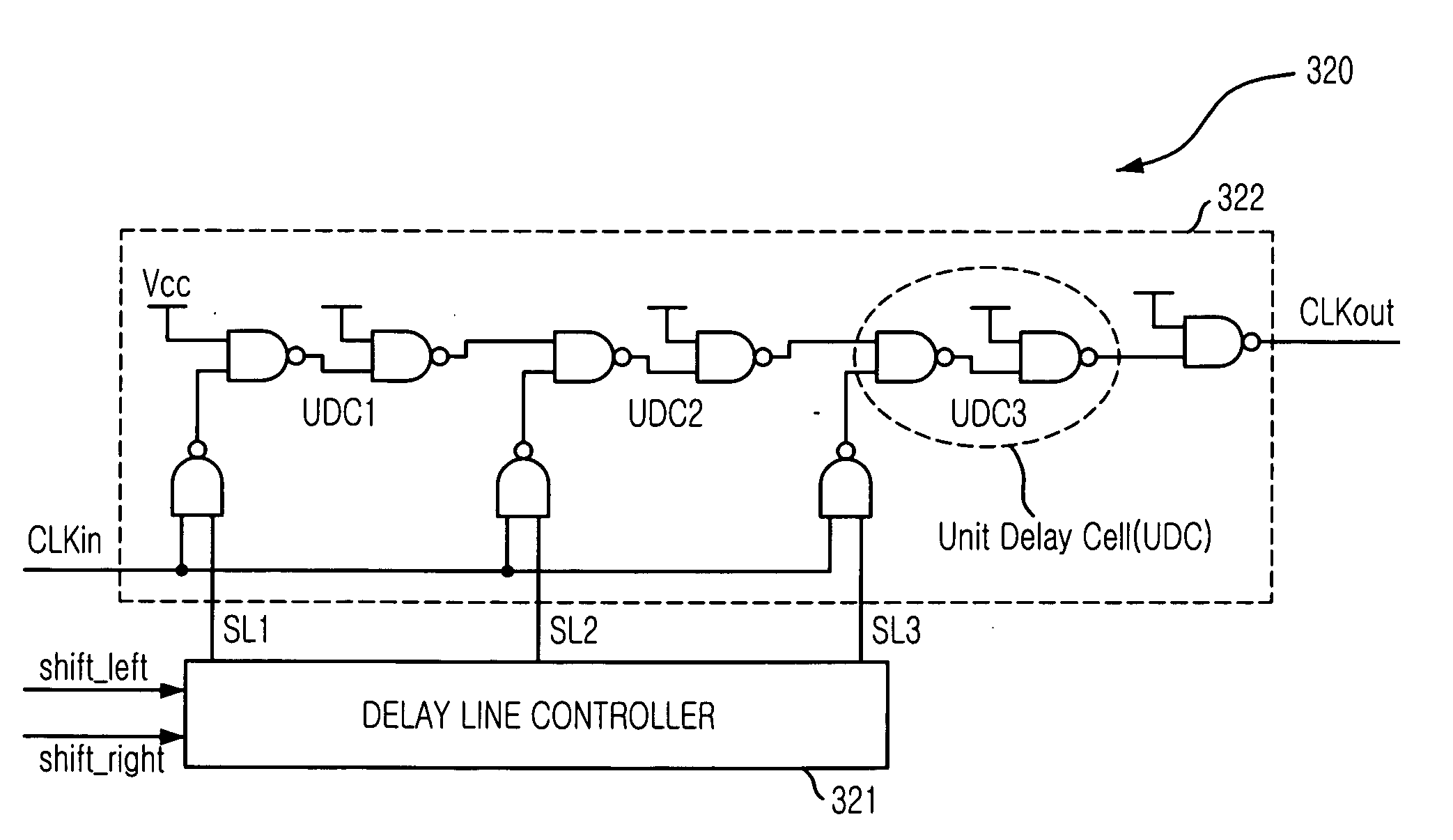
[0039]FIG. 3 is a block diagram showing a delay locked loop (DLL) in accordance with the present invention.

[0040] As shown, the DLL includes a clock multiplexing unit 310, a first direct phase detector 350, a second direct phase detector 370, a first delay model unit 340, a second delay model unit 360, a delay line unit 320, a first clock phase control unit 380, a second clock phase control unit 390 and a duty cycle correction unit 330.

[0041] The clock multiplexing unit 310 receives an external clock signal CLK and an inverted signal of the external clock signal CLK, i.e., an external clock bar signal / CLK. The clock multiplexing unit 310 selects one of the external clock signal CLK and the external clock bar signal / CLK in order to output the selected clock signal to the delay line unit 320 so that the selected clock signal can be de...


PUM


Abstract

An apparatus for adjusting a clock signal, including: a clock multiplexing unit for receiving an external clock signal, an external clock bar signal and a feed-backed clock signal in order to select one of the external clock signal and the external clock bar signal as an output signal of the clock multiplexing unit based on a result of comparing a phase of the external clock signal with a phase of the feed-backed clock signal; and a delay locked loop (DLL) for generating a duty corrected clock signal and the feed-backed clock signal in response to the output signal of the clock multiplexing unit.

Description

FIELD OF THE INVENTION [0001] The present invention relates to a delay locked loop (DLL) for compensating a clock skew between an external clock signal and an internal clock signal; and, more particularly, to a DLL capable of correcting a duty cycle of the external clock signal. DESCRIPTION OF PRIOR ART [0002] Generally, in a synchronous semiconductor memory device, data access operations such as a read operation and a write operation are performed in synchronization with rising and falling edges of an external clock signal. [0003] Since there is a time delay while the external clock signal is inputted to the synchronous semiconductor memory device in order to be used as an internal clock signal of the synchronous semiconductor memory device, a delay locked loop (DLL) is employed for synchronizing the internal clock signal with the external clock signal by compensating a clock skew between the internal clock signal and the external clock signal. [0004] As an operational speed of the...

Claims


Application Information

Patent Timeline
Patent Type & Authority Applications(United States)
IPC IPC(8): H03B19/00
CPCH03K5/1565G11C8/00G11C11/40G11C11/407
Inventor LEE, HYUN-WOOKWAK, JONG-TAE
Owner SK HYNIX INC
Why Eureka
Try Eureka