Scheme and method for testing analog-to digital converters

a digital converter and analog-to-digital converter technology, applied in the direction of code conversion, transmission system, instruments, etc., can solve the problems of high complexity of design, difficult chip testing, and over-design cost, and achieve high-precision step-ramp signals

Inactive Publication Date: 2006-01-05
NAT CHENG KUNG UNIV
View PDF9 Cites 9 Cited by
  • Summary
  • Abstract
  • Description
  • Claims
  • Application Information

AI Technical Summary

Benefits of technology

[0021] Another object of the invention is to provide a test scheme of analog-to-digital converters and method thereof. The adjustment of the power supply of the control circuit generates various amplitudes of the regulated clock signal. Adjustable amplitude of the regulated clock signal for integration overcomes the unexpected deviations of semiconductor manufacture processes for generating the high accurate step-ramp signal.

Problems solved by technology

High complex designs make the difficulty in chip testing.
As a result, chip testing cost has drastically increased and may exceed the design cost.
How to develop DFT techniques for testing converters has become an important issue.
However, for high resolution ADC testing, multiple high accurate stage stimuli (2n stimuli for n-bit ADCs) are difficult to be implemented in the chip because they exhaust large chip area.
Meanwhile, switching the reference stimuli via analog switches generates noises and spikes that influence the accuracy of reference stimuli.
Therefore it cannot be applied in the chip for high resolution converter testing.
This drawback greatly influences the accuracy of the test scheme.
The main issues in this scheme are the necessity of the DAC that always has higher resolution than that of the ADC.
If this scheme is implemented with Built-In Self-Test designs, the test signal generator and the DAC will exhaust large chip area.

Method used


Image

  • Scheme and method for testing analog-to digital converters
  • Scheme and method for testing analog-to digital converters
  • Scheme and method for testing analog-to digital converters

Examples


Embodiment Construction

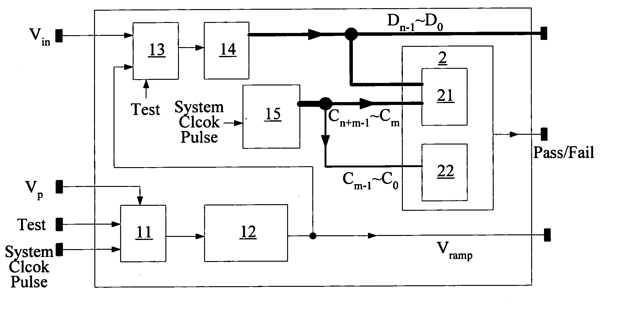
[0053] For further understanding of the test scheme, test procedure, and characters of the invention, the inventor herein presents preferred embodiment with drawings and detail descriptions.

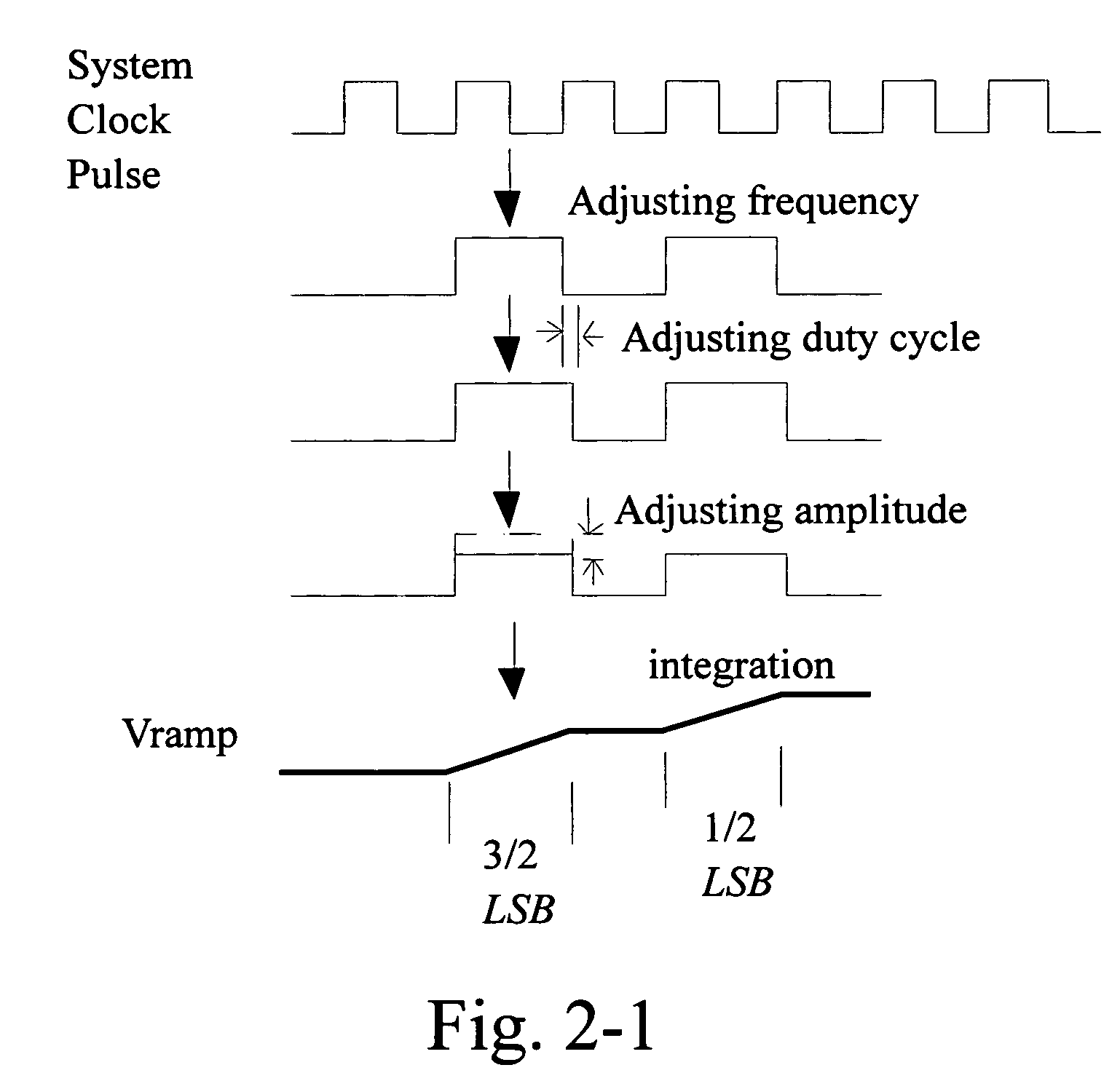
[0054]FIG. 2 illustrates the test scheme. The functions of components in the scheme are described in the following. [0055] (1) Control Circuit 11: The Control Circuit generates the regulated clock signal after the frequency, duty cycle and amplitude of the system clock pulse is regulated. Test is a trig signal. When Test=1, the test scheme is activated in test mode. Otherwise Test=0, it is in normal mode. Vp is the power source of the Control Circuit. Slightly adjusting the amplitude of the power source provides the little amplitude variation of the regulated clock signal for integration. This mechanism is designed to overcome the deviations in manufacture processes of the chips. [0056] (2) Integrator 12: It produces the step-ramp stimulus named Vramp by integrating the regulated clock signal. [...


PUM


Abstract

The invention provides a test scheme of analog-to-digital converters and method thereof. It comprises: a control circuit, a step-ramp signal generator, a multiplexer, an n+m-bit counter, and a test analyzing circuit, wherein m=1, 2, 3 . . . , based on desired accuracy of the test scheme. A clock pulse is coupled to the n+m-bit counter and a control circuit for regulating duty cycle, amplitude, and frequency. It is also coupled to a step-ramp signal generating circuit for being integrated as a test signal source. Therefore the step-ramp signal can synchronize with the n+m-bit counter, and the output codes are applied to compare with output codes of the n-bit ADCs for completely digitally analyzing ADC's parameters. The step-ramp signal is divided into several segments, each is integrated by the regulated clock signal with different duty cycles, which increases integrating time to compensate leakage currents of the capacitor and improve linearity of the step-ramp signal.

Description

BACKGROUND OF THE INVENTION [0001] 1. Field of the Invention [0002] A test scheme is invented for testing Analog-to-Digital Converters (ADCs). In this scheme, a system clock pulse is used to drive an n+m-bit counter and the frequency, duty cycle and amplitude of the system clock pulse is regulated to become a regulated clock signal that is integrated by an Integrator to form a called step-ramp signal as a test stimulus, where n is the resolution of the ADC under test and m=1, 2, 3 . . . , based on the desired accuracy of the test scheme. With this design, the step-ramp stimulus can correctly synchronize with the n+m-bit counter whose output codes provide the references for testing the n-bit ADC. The Test Response Analyzer can be designed with completely digital circuits to analyze the output codes of the ADC and the counter for identifying whether the specific parameters of the ADC are within acceptable ranges. [0003] On the other hand, the step-ramp stimulus is divided into several...

Claims


Application Information

Patent Timeline
Patent Type & Authority Applications(United States)
IPC IPC(8): H03M1/10H03M1/52
CPCH03M1/109H03M1/12H03M1/1095
Inventor WEN, YUN-CHE
Owner NAT CHENG KUNG UNIV
Why Eureka
Try Eureka