Active matrix liquid crystal display

a liquid crystal display and active matrix technology, applied in the direction of instruments, static indicating devices, etc., can solve the problems of inability to obtain sufficient display contrast, increase the aperture of pixels, and generate so as to simplify the circuit configuration thereof, the effect of removing flicker and residual images

Inactive Publication Date: 2006-01-05
LG ELECTRONICS INC
View PDF20 Cites 62 Cited by
  • Summary
  • Abstract
  • Description
  • Claims
  • Application Information

AI Technical Summary

Benefits of technology

[0010] Accordingly, it is an object of the present invention to provide a liquid crystal display apparatus and method that is adapted to eliminate flickering and residual images as well as to simplify the circuit configuration thereof.

Problems solved by technology

As a result, a flicker and a residual image are generated in the picture displayed on the liquid crystal panel.
This causes apertures of pixels to be increased, so that it is impossible to obtain a sufficient display contrast.
As a result, it is difficult to suppress the feed through voltage ΔVp sufficiently by means of the support capacitor Cst.
However, these liquid crystal display devices of scanning signal control system additionally require circuit modification of the gate driver or a new waveform modifying circuit to be positioned between the gate driver and each gate line at the liquid crystal panel.
In the liquid crystal display device of the scanning signal control system as described above, the feed through voltage ΔVp is sufficiently suppressed to reduce flickering and residual images considerably but since a waveform modifying circuit such as an integrator for each gate line must be added, the circuit configuration thereof becomes very complex.
Further, because the rising edge of the scanning signal also changes slowly due to the waveform modifying circuit, the charge initiation time at the liquid crystal cell is delayed.
Due this end, the active matrix liquid crystal display device disclosed in U.S. Pat. No. 5,587,722 consumes a large amount of power.

Method used


Image

  • Active matrix liquid crystal display
  • Active matrix liquid crystal display
  • Active matrix liquid crystal display

Examples


Embodiment Construction

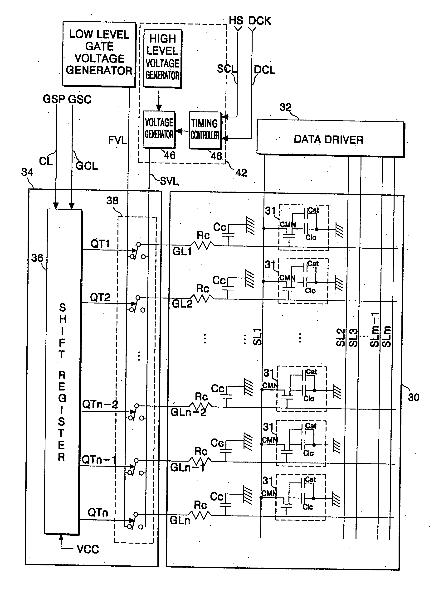
[0033] Referring to FIG. 4, there is shown an active matrix liquid crystal display device according to an embodiment of the present invention that includes a data driver 32 for driving signal lines SL1 to SLm at a liquid crystal panel 30, and a gate driver 34 for driving gate lines GL1 to GLn at a liquid crystal panel 30. In the liquid crystal panel 30, pixels 31 connected to signal lines SL and gate lines GL are arranged in an active matrix pattern. Each pixel 31 includes a liquid crystal cell Clc for responding to a data voltage signal DVS from the signal line SL to control a transmitted light quantity, and a thin film transistor (TFT) CMN for responding to a scanning signal SCS from the gate line GL to switch the data voltage signal DVS to be applied from the signal line SL to the liquid crystal cell Clc. Also, Each pixel 31 has a support capacitor Cst connected, in parallel, to the liquid crystal cell Clc. This support capacitor Cst serve to buff a voltage charged in the liquid ...


PUM


Abstract

An active matrix liquid crystal display apparatus that is adaptive for eliminating a flicker and a residual image as well as simplifying the circuit configuration thereof. In the apparatus, a plurality of pixels each includes a switching transistor having a second electrode connected to a gate electrode, a first electrode and a pixel electrode. Each of pluralities of data signal lines is connected to the second electrode associated with any one of the transistors, and each of pluralities of gate signal lines is connected to the gate electrode associated with any one of the transistors. A gate driver is connected to the plurality of gate signal lines, and it receives first and second voltages and outputs any one of the first and second voltages to drive the gate signal lines sequentially. The first voltage changes prior to exciting of successive gate signal lines.

Description

BACKGROUND OF THE INVENTION [0001] 1. Field of the Invention [0002] This invention relates to an active matrix liquid crystal display, and more particularly to an active matrix liquid crystal display wherein it is provided with a device for applying a gate pulse to transistors connected to picture elements (or pixels) consisting of liquid crystals. [0003] 2. Description of the Prior Art [0004] The conventional active matrix liquid crystal display device displays a picture by controlling the light transmissivity of liquid crystal using an electric field. As shown in FIG. 1, such a liquid crystal display device includes a data driver 12 for driving signal lines SL1 to SLm at a liquid crystal panel 10, and a gate driver 14 for driving gate lines GL1 to GLn at a liquid crystal panel 10. In the liquid crystal panel 10, pixels 11 connected to signal lines SL and gate lines GL are arranged in an active matrix pattern. Each pixel 11 includes a liquid crystal cell Clc for responding to a dat...

Claims


Application Information

Patent Timeline
Patent Type & Authority Applications(United States)
IPC IPC(8): G09G3/36
CPCG09G3/3648G09G3/3677G09G3/3696G09G2320/0247G09G2320/0219G09G2320/0223G09G2310/066
Inventor LEE, HYUN CHANG
Owner LG ELECTRONICS INC
Why Eureka
Try Eureka