

Semiconductor device and method for manufacturing the same
a technology of semiconductors and semiconductors, applied in the direction of semiconductor devices, basic electric elements, electrical equipment, etc., can solve the problem of lowering the breakdown voltag
- Summary
- Abstract
- Description
- Claims
- Application Information
AI Technical Summary
Problems solved by technology
Method used
Image

Examples
first embodiment
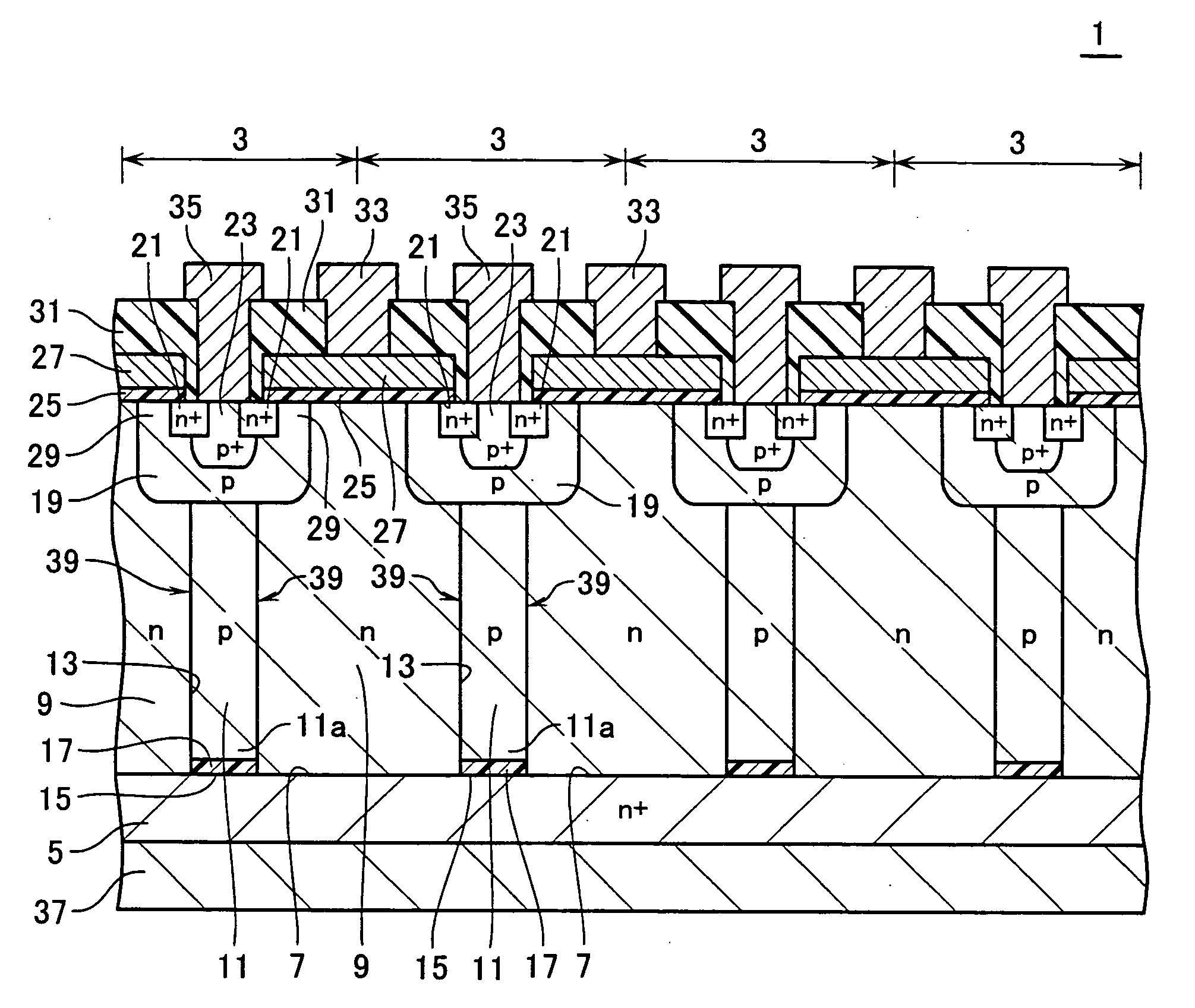
[0042] A semiconductor device according to a first embodiment has a primary characteristic in that, in the presence of insulating regions formed on bottoms in trenches, a p-type epitaxial grown layer is buried in the trenches to form second semiconductor regions as super junction-structured components.
(Structure of Semiconductor Device)
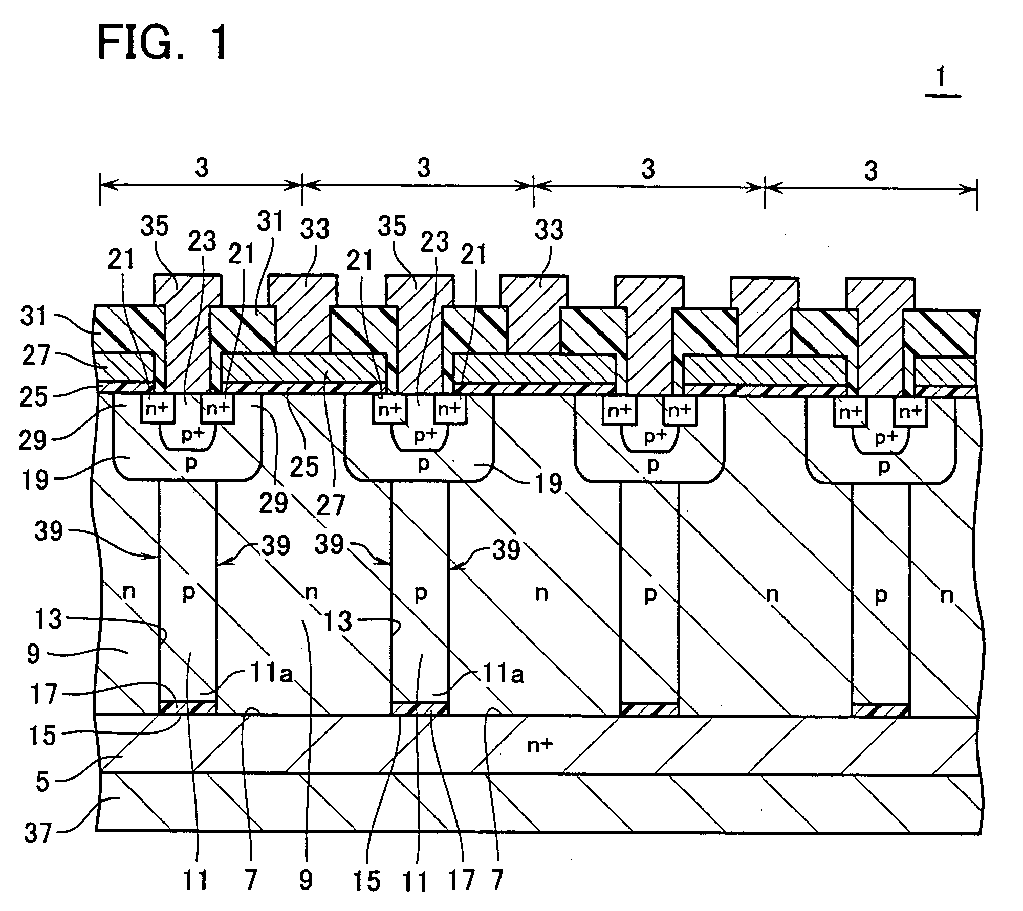
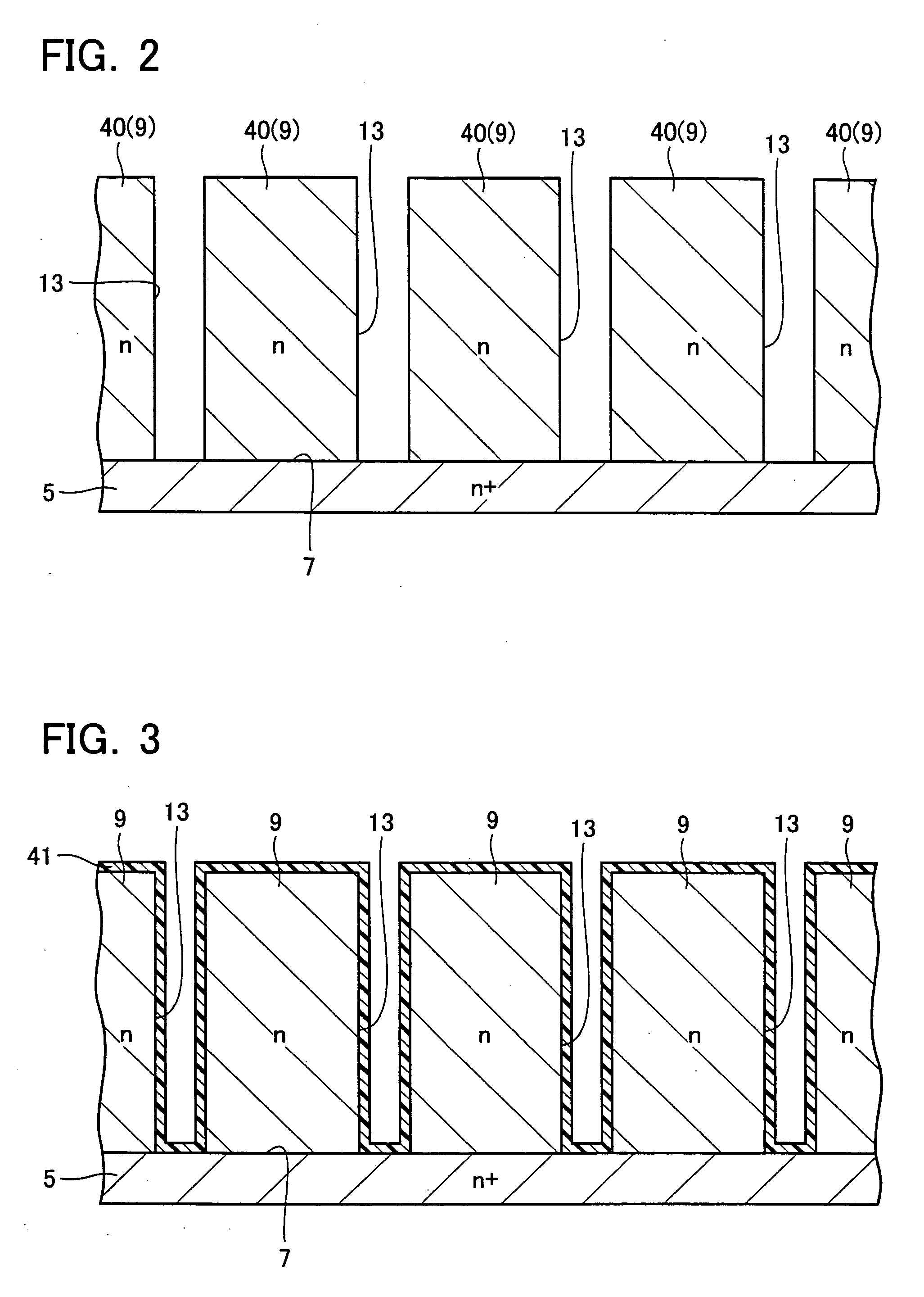
[0043]FIG. 1 is a partial cross-sectional view of the semiconductor device 1 according to the first embodiment. The semiconductor device 1 is a vertical power MOSFET structured to include a number of MOSFET cells 3 connected in parallel. The semiconductor device 1 comprises an n+-type semiconductor substrate (such as silicon substrate) 5, and a plurality of n-type first semiconductor regions 9 and a plurality of p-type second semiconductor regions 11 disposed on an upper surface 7 of the substrate. The n-type is an example of the first conduction type and the p-type is an example of the second conduction type.
[0044] The n+-type semiconductor subst...
modification 1
[0081] The modification 1 of the first embodiment is characterized in that the quantity of charge on the p-type impurity in the second semiconductor region 11 is made larger than the quantity of charge on then-type impurity in the first semiconductor region 9 in the semiconductor device 1 shown in FIG. 1. In this case, the quantity of charge on the p-type impurity in the region 11 is represented by a product of the width of the region 11 and the impurity concentration in the region. Similarly, the quantity of charge on the n-type impurity in the region 9 is represented by a product of the width of the region 9 and the impurity concentration in the region. An effect of the modification 1 is described with reference to FIG. 16 employed once to describe the effect 2 of the first embodiment.
[0082] In accordance with the modification 1, the tolerance on the unbalance between the quantities of charge on the n-type and p-type impurities can be said to lie in between 0% and +30% (not conta...
modification 2
[0083]FIG. 17 is across-sectional view of a semiconductor device 59 according the modification 2 and corresponds to FIG. 1. The semiconductor device 59 differs from the semiconductor device 1 in that the insulating region 17 has a layered structure including films of different materials. In the insulating region 17, an upper layer, which is brought into contact with the second semiconductor region 11, may be formed of an insulator film that is inactive during epitaxial growth, such as a silicon oxide film. Therefore, a lower layer than the upper layer may be formed of a different material from that of the upper layer.
[0084] The insulating region 17 of the modification 2 includes a silicon oxide film 43 serving as the upper layer and an oxygen-doped polysilicon film 61 serving as the lower layer. From the viewpoint of relieving the electric field placed across the second semiconductor region 11 as described in the effect 2, an increased thickness of the silicon oxide film 43 is desi...
PUM
 Abstract
Description
Claims
Application Information