Method and apparatus for a semiconductor device having low and high voltage transistors

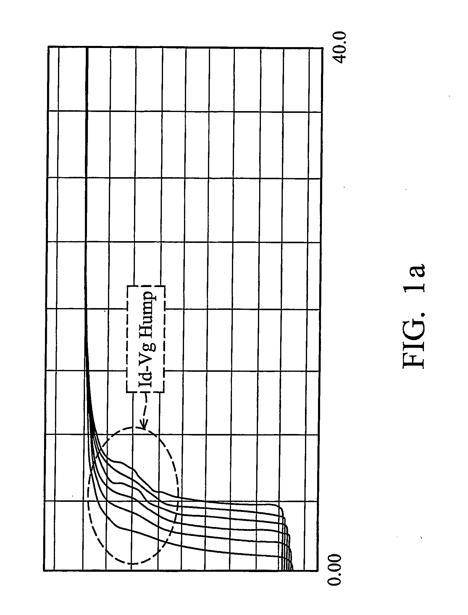
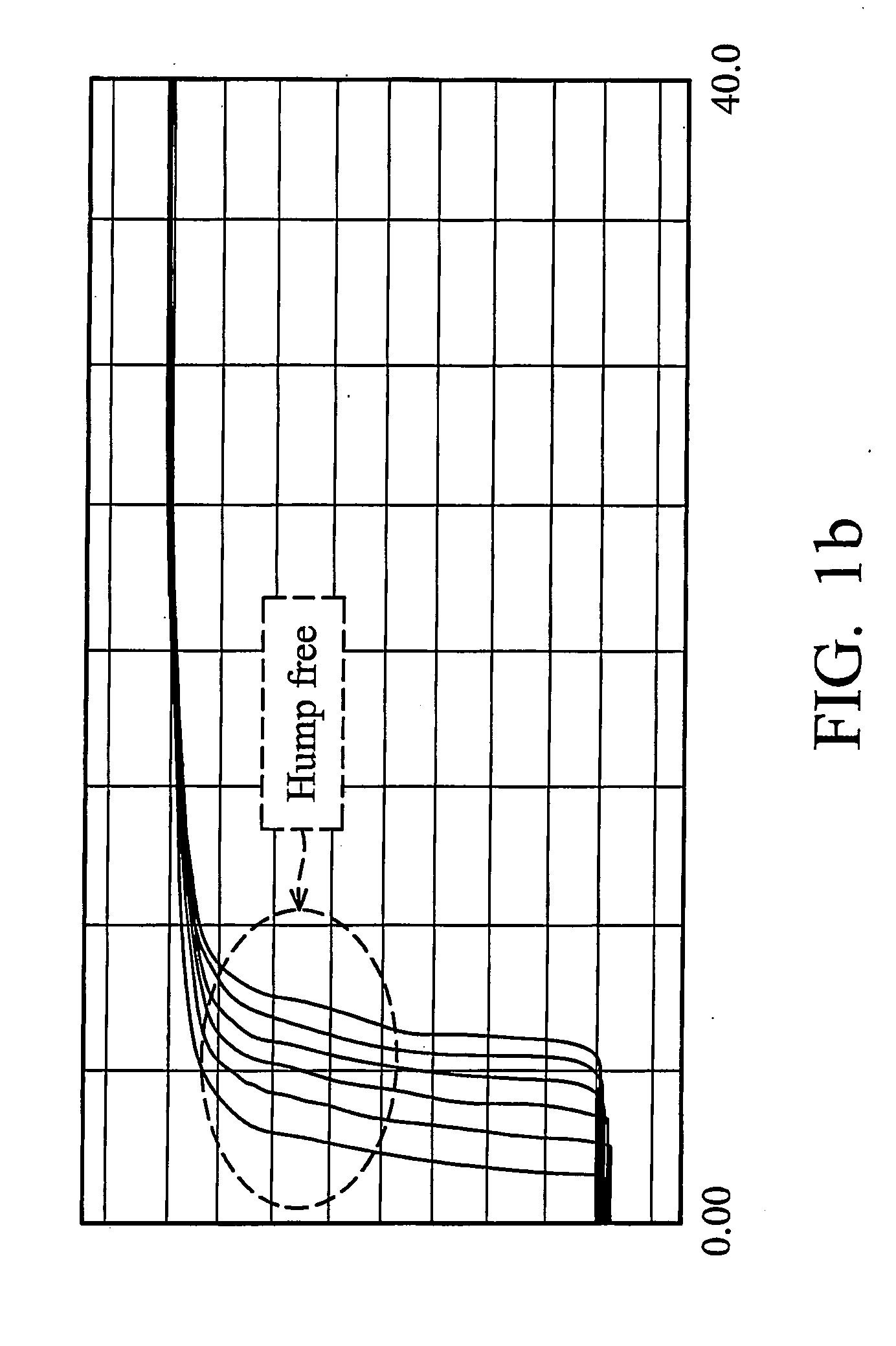
a technology of low and high voltage transistors, which is applied in the direction of semiconductor devices, electrical equipment, basic electric elements, etc., can solve the problems of low and high voltage ldmos transistors fabricated in such devices that exhibit a “hump” or undesirable discontinuity in the id (drain current) vs. the actual operation of the device deviating from the expected, designed for, operation, and the effect of reducing the number of transistors

Active Publication Date: 2006-01-12
TAIWAN SEMICON MFG CO LTD
View PDF3 Cites 54 Cited by
  • Summary
  • Abstract
  • Description
  • Claims
  • Application Information

AI Technical Summary

Benefits of technology

[0010] Various embodiments of the present invention provide a novel process and structure for a lateral double-diffused MOS (LDMOS) high voltage transistor using isolation regions with controlled active-area-to-isolation-region transition angles. In a first preferred embodiment of the structure of the invention, a buried layer is provided over a substrate, doped semiconductor wells are formed in an epitaxial layer deposited over the buried layer, isolation regions which may be shallow trench isolation regions or LOCOS regions are formed including one in a semiconductor well which will act as a drain region, gate dielectric and gate electrode material is deposited over the substrate, a patterning step is performed to form a gate electrode overlying a gate dielectric which together overly a channel region in a portion of the drain region well, and contact regions are formed to complete a source region and the drain region. The transition angle for the isolation oxide region formed within the high voltage drain well is different from, and less abrupt, than the transition angle of isolation regions formed elsewhere in the substrate.

Problems solved by technology

In the prior art, a problem which arises particularly with such SOC integrated circuits including both low and high voltage MOS devices in a single piece of silicon substrate is that the high voltage LDMOS transistors fabricated in such devices often exhibit a “hump” or undesirable discontinuity in the Id (drain current) vs.
This Id-Vg “hump” is an undesirable electrical characteristic and results in less than desirable performance, or even unacceptable performance, in the completed devices.
That is, the actual operation of the devices deviates from the expected, and designed for, operation.

Method used


Image

  • Method and apparatus for a semiconductor device having low and high voltage transistors
  • Method and apparatus for a semiconductor device having low and high voltage transistors
  • Method and apparatus for a semiconductor device having low and high voltage transistors

Examples


Embodiment Construction

[0035] The operation and fabrication of the presently preferred embodiments are discussed in detail below. However, the embodiments and examples described herein are not the only applications or uses contemplated for the invention. The specific embodiments discussed are merely illustrative of specific ways to make and use the invention, and do not limit the scope of the invention or the appended claims.

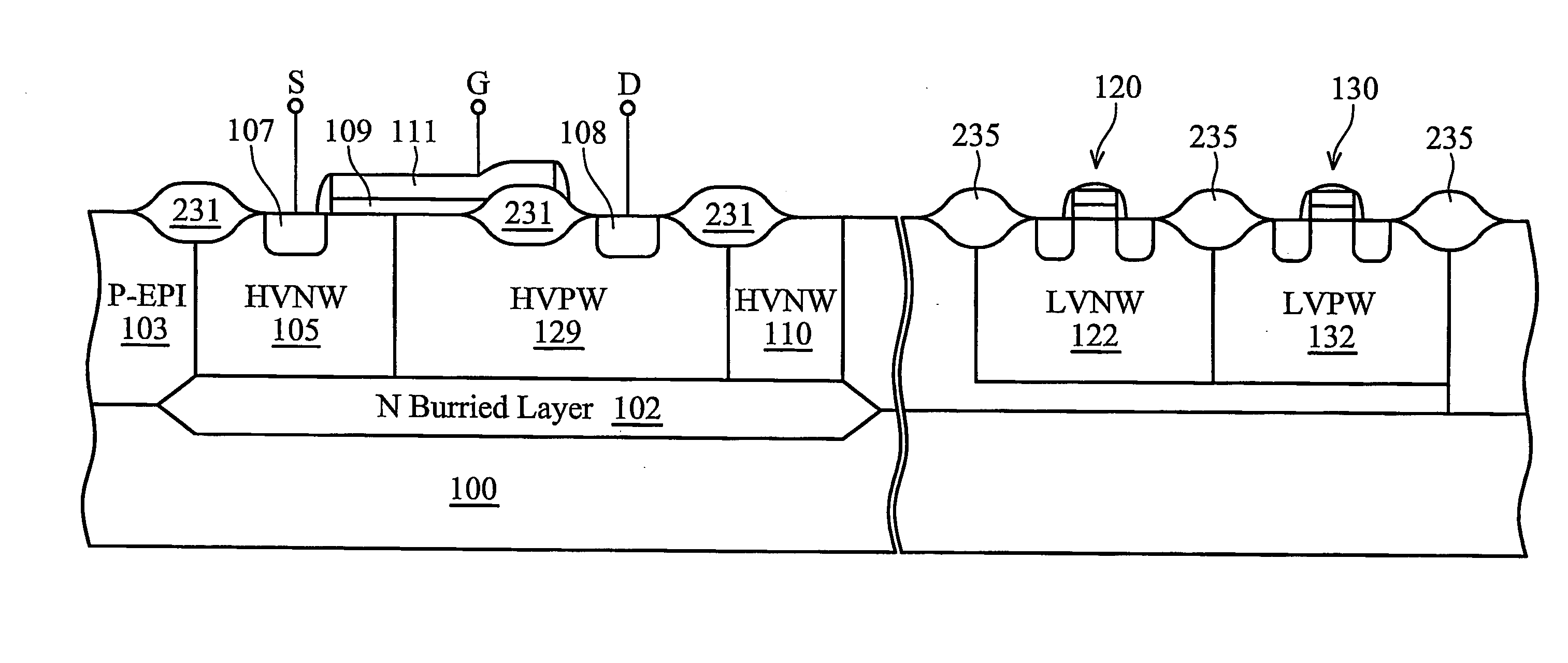
[0036]FIG. 2 depicts in a simplified cross sectional view, drawn in a representational view and not to scale, a portion of an integrated circuit having a single exemplary high voltage transistor and two exemplary lower voltage transistor disposed in a high voltage and a low voltage region. A practical circuit would have many of each type of transistor, perhaps thousands of each. During fabrication of the devices as described in more detail below, masking including photoresist or nitride hard masks will be used to asymmetrically process the high voltage and low voltage regions when ne...


PUM


Abstract

Method and apparatus for a semiconductor device including high voltage MOS transistors is described. A substrate is provided with a low voltage and a high voltage region separated one from the other. Isolation regions containing an insulator are formed including at least one formed within one of said wells within the high voltage region. The angle of the transition from the active areas to the isolation regions in the high voltage device region is greater than a predetermined angle, in some embodiments it is greater than 40 degrees from vertical. In some embodiments the isolation regions are formed using shallow trench isolation techniques. In alternative embodiments the isolation regions are formed using field oxide formed by local oxidation of silicon techniques.

Description

[0001] This application claims priority to provisional patent application Ser. No. 60 / 587,677, filed Jul. 12, 2004, entitled “Method for Controlling High Voltage Device Id-Vg Curve Characteristic by Controlling the STI Transition Angle and Circuit Constructed Thereby”, which application is hereby incorporated herein by reference.TECHNICAL FIELD [0002] The present invention and the various embodiments described generally relate to the fabrication of semiconductor devices including power transistors, and more particularly to fabricating integrated devices which incorporate at least one high voltage lateral DMOS transistor also having an isolation region disposed between a source and a drain region. BACKGROUND [0003] In the semiconductor art, it is desirable to improve transistor performance even as devices become smaller due to ongoing reductions in device scale. Further, it is desirable to manufacture integrated circuit semiconductor devices that incorporate transistors for low, high...

Claims


Application Information

Patent Timeline
Patent Type & Authority Applications(United States)
IPC IPC(8): H01L29/76
CPCH01L21/76229H01L21/76232H01L21/82385H01L21/823857H01L29/7816H01L29/42368H01L29/66681H01L29/7391H01L29/0653
Inventor CHANG, CHI-HSUENLIU, JUN XIUHUANG, TSUNG-YICHEN, CHUNG-ISUNG, TZU-CHIANGHUANG, CHIH POYEH, RANN SHYAN
Owner TAIWAN SEMICON MFG CO LTD
Why Eureka
Try Eureka