Nanowire device with (111) vertical sidewalls and method of fabrication

a technology of nanowires and sidewalls, applied in the field of nanowire fabrication, can solve the problems of crystal degradation, slow e-beam lithography, limited use in high throughput or production situations,

Inactive Publication Date: 2006-01-12
HEWLETT PACKARD DEV CO LP
View PDF11 Cites 68 Cited by
  • Summary
  • Abstract
  • Description
  • Claims
  • Application Information

AI Technical Summary

Problems solved by technology

However, e-beam lithography is slow and therefore of limited use in high throughput or production situations.
Moreover, e-beam lithography has limited resolution in the nano-scale range.
While nano-imprinting is viable, the RIE process used therewith causes crystal degradation, introduces surface roughness in the sidewalls of the patterns, and uses a metal mask that contaminates the nano-structures with metal ions.
Moreover, the conventional RIE process tends to impose limitations on the dimensions of the fabricated nano-structures.
Whether used with e-b

Method used


Image

  • Nanowire device with (111) vertical sidewalls and method of fabrication
  • Nanowire device with (111) vertical sidewalls and method of fabrication
  • Nanowire device with (111) vertical sidewalls and method of fabrication

Examples


Embodiment Construction

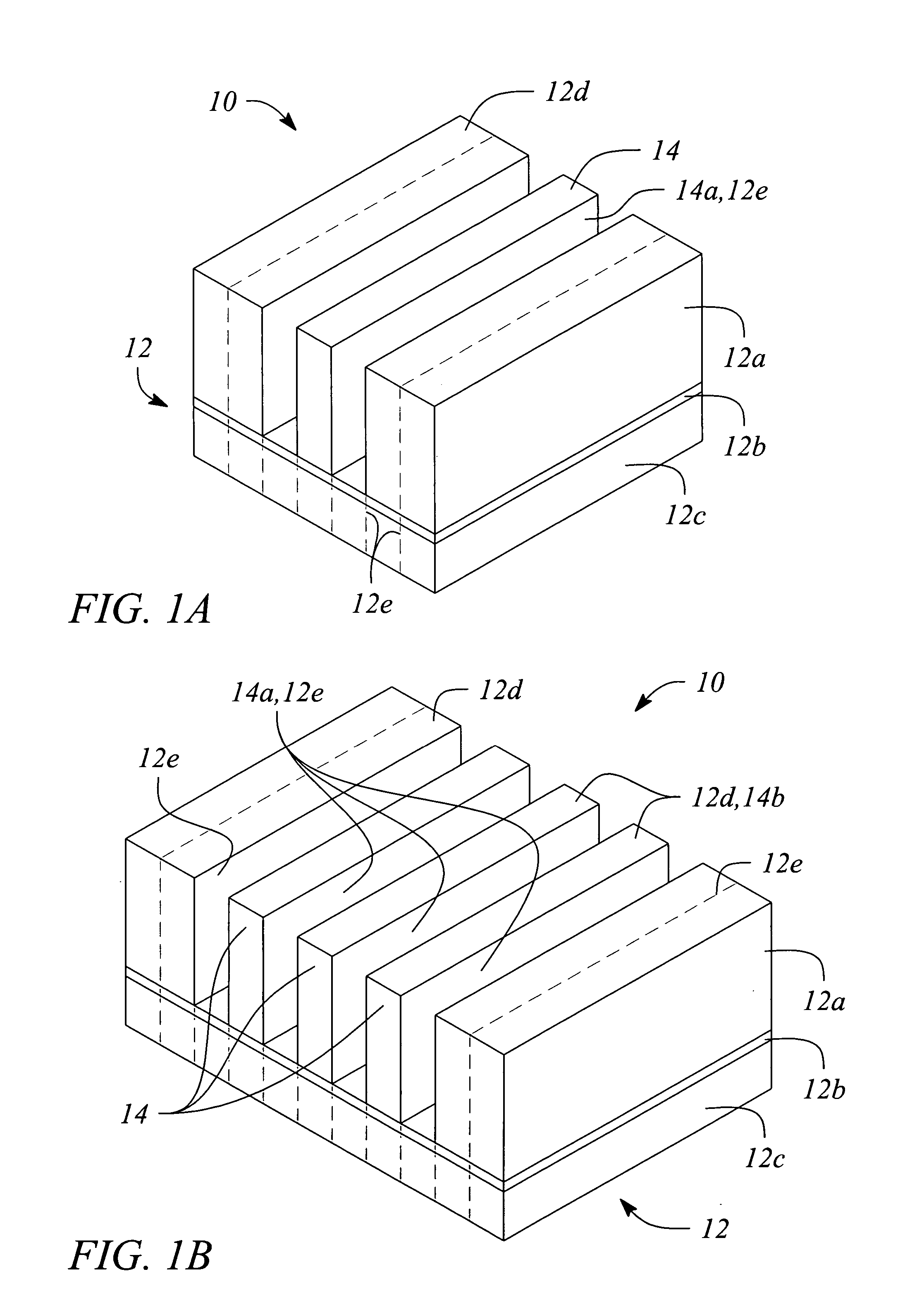
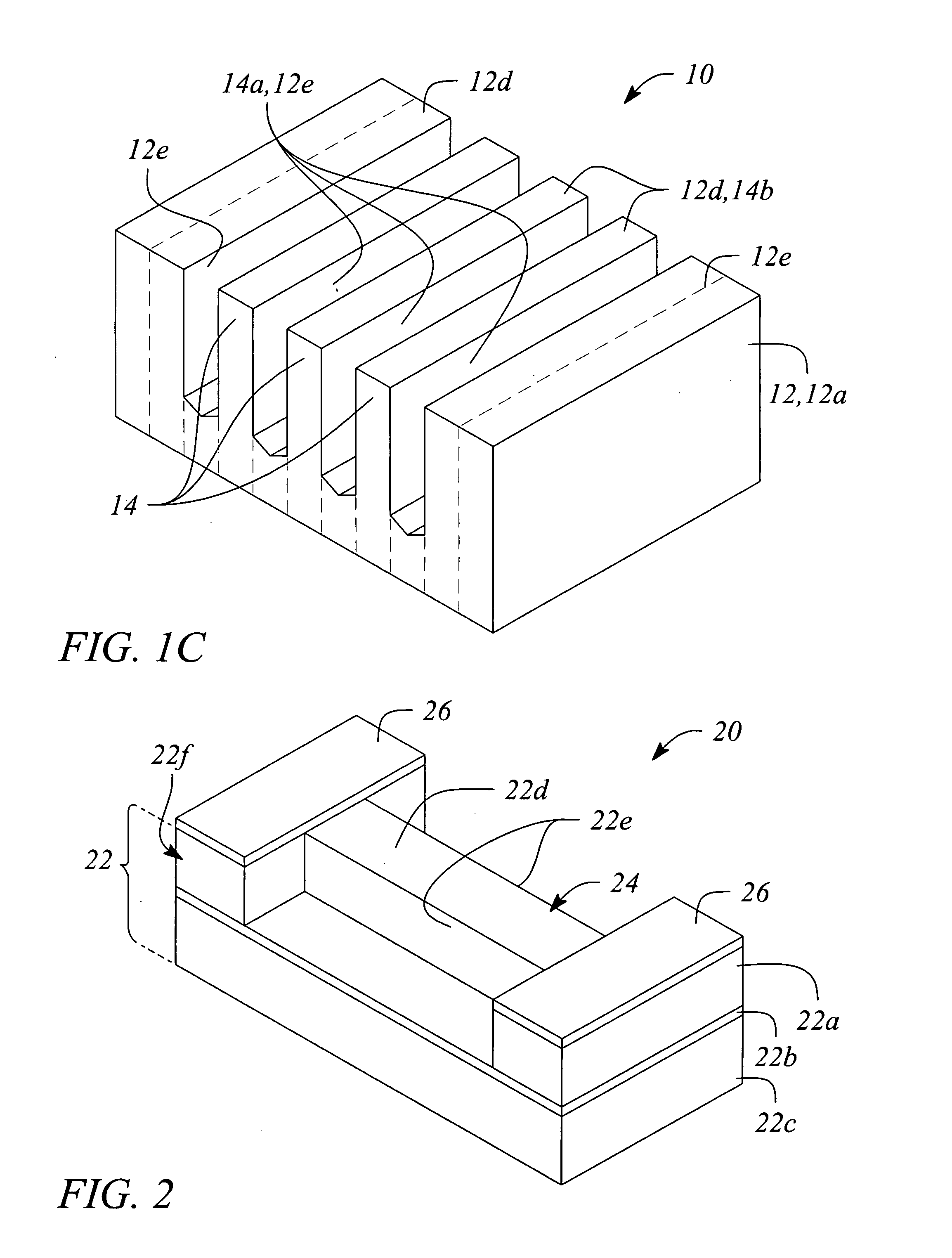
[0022]FIGS. 1A-1C illustrate a perspective view of embodiments of a nano-scale structure 10 in accordance with an embodiment of the present invention. The nano-scale structure 10 comprises a semiconductor substrate 12 that is polished in a [110] direction, and a semiconductor nanowire 14 wet chemically etched in the semiconductor layer 12a.

[0023] The semiconductor substrate 12 is either a semiconductor wafer 12, 12a or a semiconductor-on-insulator wafer 12. The semiconductor-on-insulator wafer 12 comprises a semiconductor layer 12a adjacent to an insulator layer 12b and a remainder support material 12c of the wafer 12 adjacent to the insulator layer 12b, as illustrated in FIGS. 1A and 1B. The semiconductor wafer 12, 12a is illustrated in FIG. 1C. Therefore, the term ‘semiconductor layer’ is used herein to mean either a semiconductor wafer 12, 12a or a semiconductor-on-insulator wafer 12 having a semiconductor layer 12a, unless otherwise specified.

[0024] By [110] direction, it is m...


PUM


Abstract

A nano-scale device and method of fabrication provide a nanowire having (111) vertical sidewalls. The nano-scale device includes a semiconductor-on-insulator substrate polished in a [110] direction, the nanowire, and an electrical contact at opposite ends of the nanowire. The method includes wet etching a semiconductor layer of the semiconductor-on-insulator substrate to form the nanowire extending between a pair of islands in the semiconductor layer. The method further includes depositing an electrically conductive material on the pair of islands to form the electrical contacts. A nano-pn diode includes the nanowire as a first nano-electrode, a pn-junction vertically stacked on the nanowire, and a second nano-electrode on a (110) horizontal planar end of the pn-junction. The nano-pn diode may be fabricated in an array of the diodes on the semiconductor-on-insulator substrate.

Description

BACKGROUND [0001] 1. Technical Field [0002] The invention relates to nanotechnology and the fabrication of nano-scale structures. In particular, the invention relates to fabrication of a nanowire and a device having a nanowire using wet chemical etching. [0003] 2. Description of Related Art [0004] A consistent trend in semiconductor technology since its inception is toward smaller and smaller device dimensions and higher and higher device densities. As a result, an area of semiconductor technology that recently has seen explosive growth and generated considerable interest is nanotechnology. Nanotechnology is concerned with the fabrication and application of so-called nano-scale structures, structures having dimensions that are often 50 to 100 times smaller than conventional semiconductor structures. Typically, either e-beam patterning or nano-imprinting combined with dry etching, such as reactive ion etching (RIE), are techniques used to fabricate nano-scale structures. [0005] Howev...

Claims


Application Information

Patent Timeline
IPC IPC(8): H01L27/01H01L21/00
CPCB82Y10/00G11C2213/81H01L27/1203H01L29/861H01L29/0665H01L29/0673H01L29/045H01L21/306B82B3/00
Inventor ISLAM, M. SAIFCHEN, YONGWANG, SHIH-YUANWILLIAMS, R. STANLEY
Owner HEWLETT PACKARD DEV CO LP
Why Eureka
Try Eureka