
Mask and inspection method therefor and production method for semiconductor device

a technology of semiconductor devices and inspection methods, applied in the direction of originals for photomechanical treatment, instruments, optics, etc., can solve the problems of affecting the quality of the product, the pattern is not printed accurately, and the membrane may be damaged

Inactive Publication Date: 2006-01-12
SONY CORP
View PDF10 Cites 22 Cited by
  • Summary
  • Abstract
  • Description
  • Claims
  • Application Information

AI Technical Summary

Benefits of technology

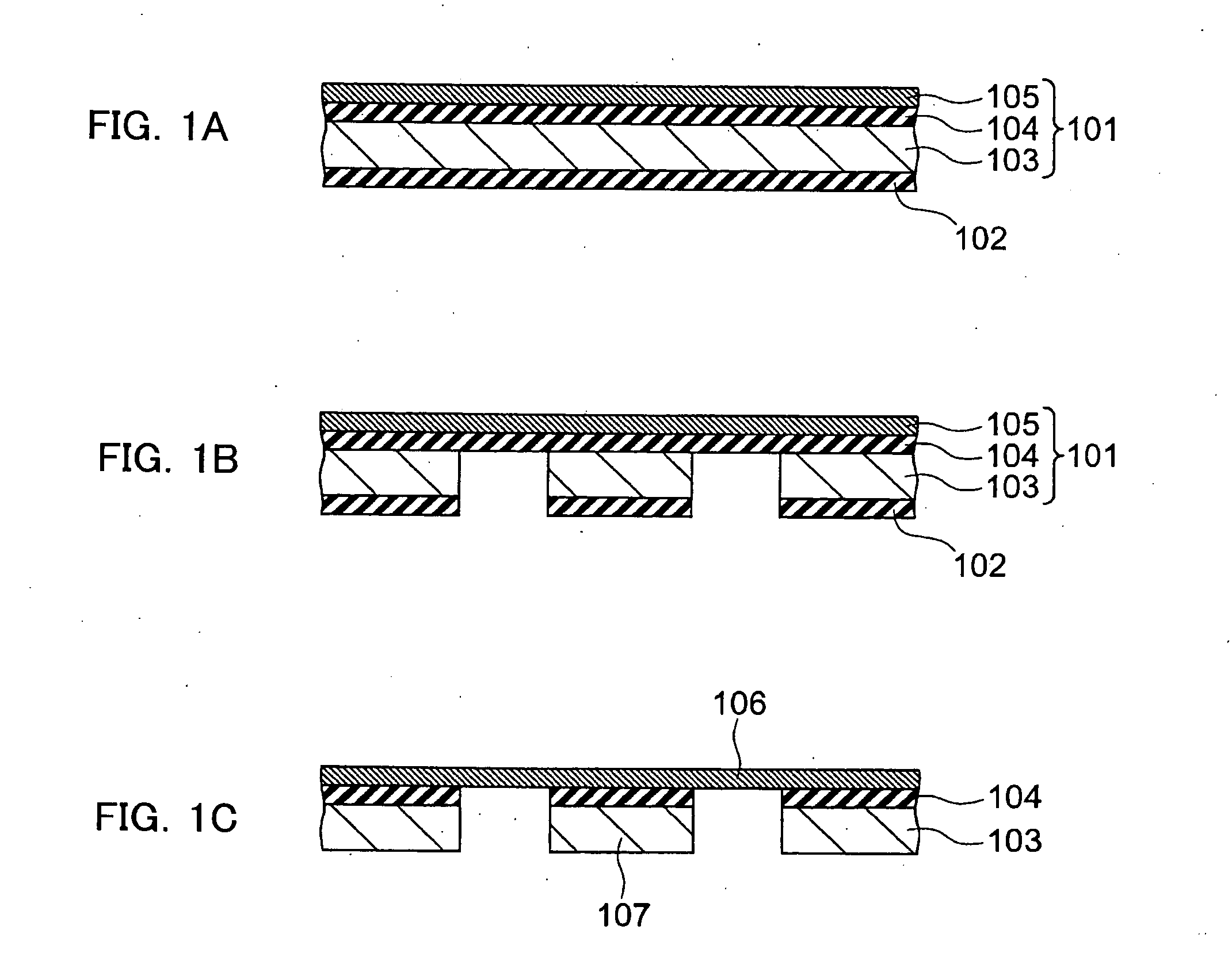
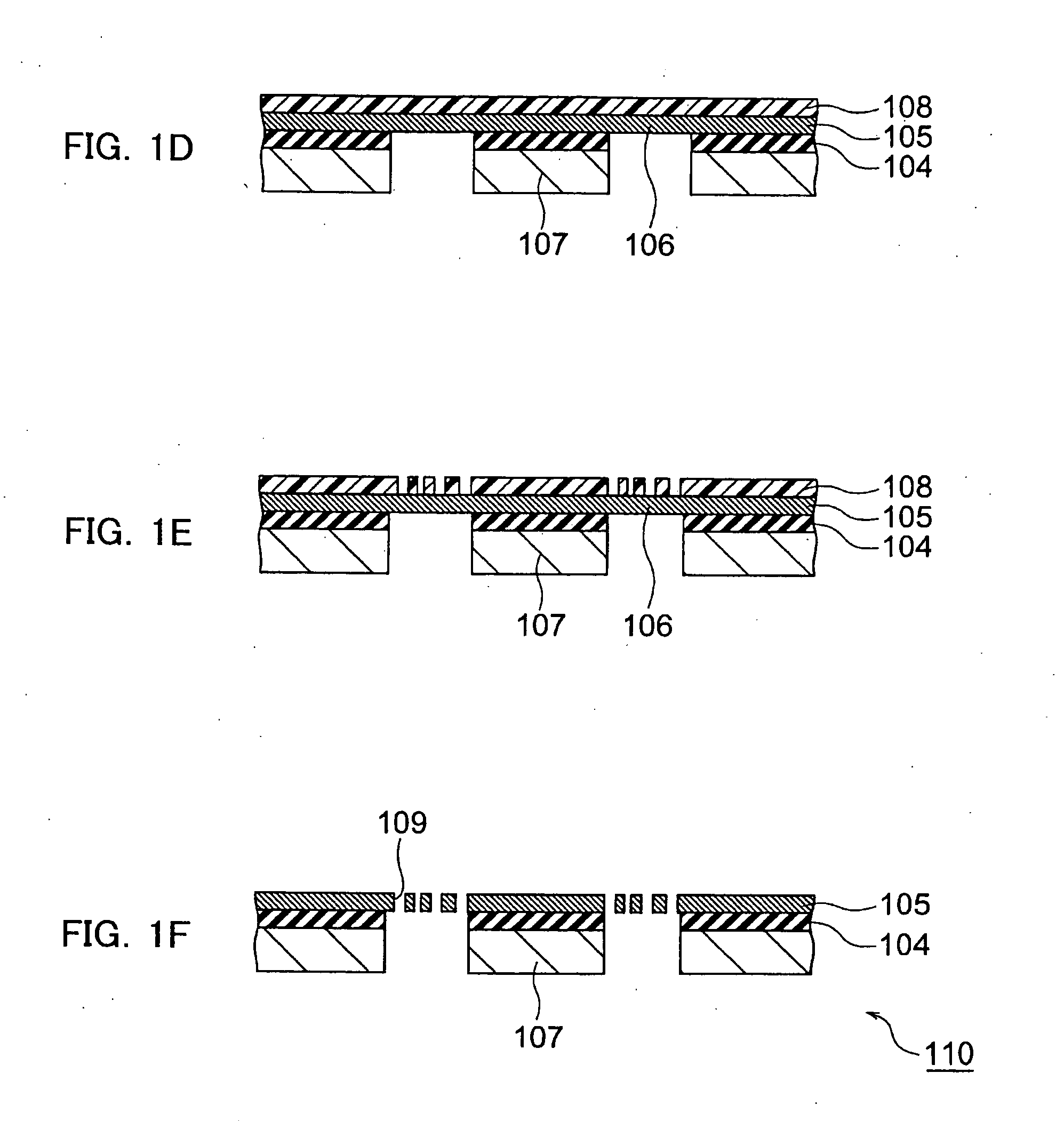
[0026] The present invention was made in consideration of said problems, therefore the object of the present invention is to produce the mask being possible to perform the destructive inspection without making the mask for the inspection or to perform more accurately the non-destructive inspection, or to produce the method of producing the mask.
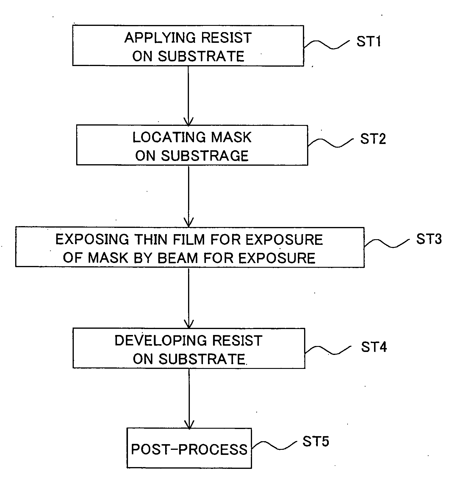
[0027] In addition, the present invention is possible to perform the mask inspection such as the destructive inspection and so on by using the mask for exposure, the object of the present invention is to produce the method of manufacturing the semiconductor device being possible to reduce pagination of making the mask.
[0034] Herewith, even inspection with destruction of a pattern can be possible to perform with a mask used for exposure. Moreover, since to perform inspection about a transmission portion formed in a step identical to a transmission portion used for exposure actually can be possible, to evaluate more accurately a condition of a transmission portion used for exposure.
[0036] According to a method of producing a semiconductor device of the present invention using a mask of the present invention, since a mask of-the present invention that a condition of a thin film for exposure can be comprehended by a thin film for inspection for lithography, TAT, that is to say turn around time, of producing a mask is reduced in producing a semiconductor device and the cost is also reduced.

Problems solved by technology

Moreover, in the case of the stencil mask, since internal stress at the portion of the aperture becomes zero, depending on the pattern the stress concentration occurs in a portion of the membrane, there is a possibility that the membrane may be damaged.
Moreover, in the case of not processing the wall surface vertically, the thickness of the mask does / not become uniform adjacent to the wall surface, the possibility that an electron beam and so on passing through the portion except the aperture may arise.
Therefore, the pattern is not printed accurately.
Therefore, in particular in the portion being formed a microscopic pattern, because the mechanical intensity of the mask is insufficient, the pattern is likely to be damaged.
For example, if physical impact is added to the mask at a deportation in producing or using the mask, using the mask is impossible by destructing the pattern.
Even if a damage of the pattern at a permissible degree, using the mask becomes impossible by accumulating the damage in repeat of using, cleaning and deporting the mask and by occurring to a critical destruction.
For performing the inspection with destroying the mask pattern, it is necessary to make a simulated mask for inspection, in other words a dummy mask, in the identical condition to the mask used actually, increasing the cost has become problematic.

Method used


Image

  • Mask and inspection method therefor and production method for semiconductor device
  • Mask and inspection method therefor and production method for semiconductor device
  • Mask and inspection method therefor and production method for semiconductor device

Examples


embodiment 1

[0052] This embodiment relates to a method of monitoring internal stress of a membrane using a mask of the present invention. For the method of measuring internal stress of a membrane constructing the stencil mask, two methods such as (1) a method of measuring flexure of the membrane and calculating internal stress based on quantity of flexure, and (2) a method of measuring internal stress directly, are considered.

[0053] In the case that internal stress of the membrane is not adjusted adequately for the stencil mask, the membrane flexes, and accuracy of position of the pattern is reduced. Alternatively for a proximity exposure method such as LEEPL, if the flexure of the membrane increases, the membrane and the wafer are in touch, hence there is the possibility that the mask is destroyed.

[0054] Therefore, by using the membrane for inspection 4 shown in FIG. 4, quantity of flexure of the membrane is surveyed, this method is, that is to say, the method of said (1). By performing this...

embodiment 2

[0067] This embodiment relates to a method of inspecting a cross sectional shape by using a mask of the present invention. In this embodiment, a pattern suitable for observation of a cross sectional shape is located on a membrane for inspection 4 of a stencil mask shown FIG. 4. An example of such a pattern is shown in FIG. 6A and FIG. 6B.

[0068]FIG. 6A is a view that the membrane for inspection 4 in FIG. 4 is enlarged, FIG. 6B is a view that a portion of the membrane for inspection 4 in FIG. 6A is enlarged. As shown in FIG. 6A and FIG. 6B, as a pattern for observation of a cross sectional shape, for example a line-and-space pattern 6 having a line width of 200 nm and a pitch of 400 nm in a region of 1 by 1 μm square. A process that an aperture is formed with the line-and-space pattern 6 on the membrane for inspection 4 is identical to a process that an aperture is formed with a predetermined pattern on the membrane for exposure 2.

[0069] Next, by irradiating a portion of the membran...

embodiment 3

[0073] This embodiment relates to method of inspecting line width uniformity and in-plane uniformity by using a mask of the present invention. Line width uniformity and in-plane uniformity of the pattern formed in an etching process change depending on line width or density of the pattern. A phenomenon that an etching speed shows a dependence on an etching area and an etching speed lowers as an etching area increases is called the loading effect.

[0074] Moreover, a phenomenon that an etching speed lowers as a line width of a pattern, in other words a diameter of an aperture, is reduced and a phenomenon that an etching speed does not become uniform when a pattern having an identical line width exists at different density are called micro-loading effect.

[0075] A membrane of a stencil mask and a scatterer of a charged particle beam of a scattering membrane mask are processed by an etching that a resist is used as a mask. Therefore, except for a line width fluctuation arising from the ...


PUM

PropertyMeasurementUnit
thicknessaaaaaaaaaa
widthaaaaaaaaaa
widthaaaaaaaaaa

Abstract

To provide a mask that it becomes possible to perform destructive inspection without a mask for inspection or to perform more accurately non-destructive inspection and a method of inspecting the same. A mask comprising a thin film for exposure that has a transmission portion and a non-transmission portion of a beam for exposure, a thick film portion that is formed around the thin film for exposure and that supports the thin film for exposure, and a thin film for inspection that has a transmission portion and a non-transmission portion of the beam for exposure, that is formed at a distance from a thin film for exposure and that has thickness and material equal to those of a thin film for exposure, and a method of inspection of a mask that inspection is performed by using a thin film for inspection, and a method of producing a semiconductor device that lithography is performed by using a thin film for exposure of the mask.

Description

TECHNICAL FIELD [0001] The present invention relates to a mask being used at the lithography process in producing of a semiconductor device, a method of inspecting the same, and a method of producing the semiconductor device. BACKGROUND ART [0002] As an alternative exposing technology of a next generation to photolithography, a printing type exposing technology using a charge particle such as an electron beam (strut) or an ion beam has being developed. In these new technology mutually, the mask having a thin film region, in other words a membrane, is used. The membrane on the surface of the mask has the thickness of about 100 nm to 10 μm, a printing pattern is placed on the membrane. The membrane is formed by etching a mask material, for example containing a silicon wafer, in part from the reverse side of the mask. A portion without etching of a mask blanks becomes a supporting portion of the membrane. [0003] The thing that the printing pattern is formed by setting an aperture at th...

Claims


Application Information

Patent Timeline
Patent Type & Authority Applications(United States)
IPC IPC(8): G03F1/00G03C5/00G06K9/00G03F1/20G03F1/84H01L21/027
CPCG03F1/20G03F1/84G03F1/44G03F1/74
Inventor WATANABE, YOKOOMORI, SHINJIIWASE, KAZUYAYOSHIZAWA, MASAKI
Owner SONY CORP
Learn More