Apparatus for manufacturing electronic device, method of manufacturing electronic device, and program for manufacturing electronic device

a technology for electronic devices and manufacturing methods, applied in lighting and heating apparatus, charge manipulation, furniture, etc., can solve problems such as affecting productivity improvement, reflow cracks may be generated in bonding parts, and solder bonding through solder paste may not be carried out well, so as to suppress the circumferential dissipation of heat, accurately control the temperature profile, and control the heating condition of the area

Inactive Publication Date: 2006-01-12
SEIKO EPSON CORP
View PDF14 Cites 18 Cited by
  • Summary
  • Abstract
  • Description
  • Claims
  • Application Information

AI Technical Summary

Benefits of technology

[0014] By doing so, it is possible to easily control the heating condition of the area to be heated and to easily change the heating position of the area to be heated by controlling the distance between the area to be heated and the heat generating means.
[0043] By doing so, even when the product pitches of the circuit blocks are different from each other, it is possible to appropriately control the distance between the area of the continuous body to be heated and the heat generating means, and to efficiently manufacture various electronic devices while suppressing the thermal damage in reflow.

Problems solved by technology

Here, during the reflow process, if peak heat is suddenly applied, reflow cracks may be generated in a bonding member such as an adhesive between the tape substrate 101 and a semiconductor chip or the semiconductor chip itself, or solder bonding through the solder paste may not be carried out well.
However, in the method of matching the processing time in each heater zone 111 to 113 to each product pitch, every time the product pitches are different, the processing time in each heater zone 111 to 113 has to be set, thus hindering improvements in productivity.
Furthermore, for example, spot heating may be carried out in correspondence with each product pitch by employing a laser heating method, but since the heating process using laser heating is partial, the heating cannot be carried out on several units simultaneously.

Method used


Image

  • Apparatus for manufacturing electronic device, method of manufacturing electronic device, and program for manufacturing electronic device
  • Apparatus for manufacturing electronic device, method of manufacturing electronic device, and program for manufacturing electronic device
  • Apparatus for manufacturing electronic device, method of manufacturing electronic device, and program for manufacturing electronic device

Examples


first embodiment

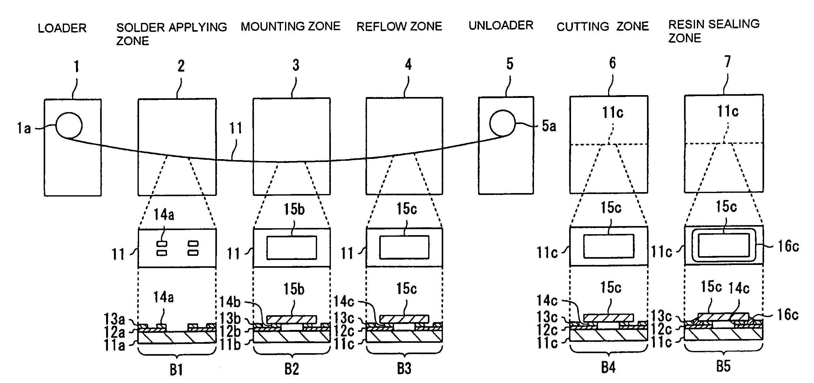
[0053]FIG. 1 is a view illustrating a method for manufacturing an electronic device in accordance with the present invention.

[0054] In FIG. 1, a solder applying zone 2, a mounting zone 3, and a reflow zone 4 are sequentially aligned in the transport direction of a tape substrate 11 between a loader 1 and an unloader 5.

[0055] In addition, on the tape substrate 11, electronic component mounting areas are provided on every circuit block B1 to B3, and each circuit block B1 to B3 is provided with circuit substrates 11a to 11c. Each wiring 12a to 12c is formed on each circuit substrate 11a to 11c, the terminal portions of the wirings 12a to 12c are exposed, and each insulating film 13a to 13c is formed on each wiring 12a to 12c.

[0056] The tape substrate 11, on which the circuit substrates 11a to 11c having predetermined lengths are arranged in a line, extends between an unwinding reel 1a and a take-up reel 5a. In each transport tact of the tape substrate 11, a solder non-applied zone of...

second embodiment

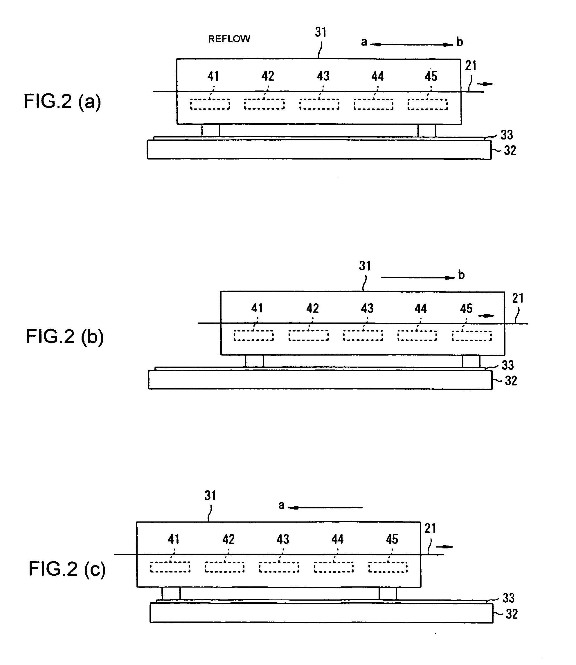
[0062]FIG. 2 is a side view illustrating an apparatus for manufacturing an electronic device in accordance with the present invention.

[0063] Referring to FIG. 2(a), a reflow furnace 31 is supported by a supporting stand 32 having a rail 33. For example, the heating process and the cooling process are performed for the circuit substrate as a body to be heated, which is placed in a line on the tape substrate 21 in the reflow process performed after the soldering process and the mounting process. The reflow furnace 31 is provided with heater zones 41 to 44 which raise the temperature of the circuit substrate step-by-step and a cooling zone 45 which performs a cooling process to lower the temperature of the circuit substrate. In addition, the reflow furnace 31 can simultaneously or separately perform the above process for a plurality of the circuit substrates which are placed in a line on the tape substrate 21.

[0064] In addition, as shown in FIGS. 2(b) and (c), the reflow furnace 31 ca...

third embodiment

[0065]FIG. 3 is a view illustrating a method for manufacturing an electronic device in accordance with the present invention and FIG. 4 is a view illustrating a temperature profile of the reflow process of FIG. 3.

[0066] In FIGS. 3 and 4, the reflow furnace 61 can be moved along a transport direction of a tape substrate 50, and the reflow furnace 61 is provided with heater zones 71 to 74 and a cooling zone 75. A circuit substrate 51 is placed in a line on the tape substrate 50 as a continuous body which is carried along the right arrow direction in a predetermined tact. In the circuit substrate 51, a solder paste 54 is attached on a wiring 52 in the soldering process before the reflow process. In addition, an adhesive such as ACF can be attached on the wiring 52 by means of a transfer method. Reference numeral 54 indicates an insulating film. In the mounting process after the soldering process, the semiconductor chip 55 is mounted on the circuit substrate 51 through the solder paste ...


PUM

PropertyMeasurementUnit
lengthaaaaaaaaaa
lengthaaaaaaaaaa
lengthaaaaaaaaaa

Abstract

A reflow process is provided for multiple units which improves productivity. A reflow furnace is moved along a transport direction of a tape substrate and is fixed at a position matching the product pitch of a circuit substrate. Any of a plurality of heating blocks and cooling blocks are matched to the product pitches of the circuit substrate. By doing so, it is possible to continuously carry out the reflow process for a tape substrate on which circuit substrates having different product pitches are arranged.

Description

CROSS REFERENCE TO RELATED APPLICATIONS [0001] This application is a divisional application of U.S. Ser. No. 10 / 394,493 filed Mar. 21, 2003 and claims priority to Japanese Application No. 2002-081223 filed Mar. 22, 2002 and Japanese Application No. 2003-024651 filed Jan. 31, 2003, all of which are incorporated by reference.BACKGROUND [0002] 1. Technical Field of the Invention [0003] The present invention relates to an apparatus for manufacturing an electronic device, a method of manufacturing an electronic device, and a program for manufacturing an electronic device, which are specifically applicable to a solder reflow process by which electronic components are mounted on a tape substrate. [0004] 2. Description of the Related Art [0005] In manufacturing a semiconductor device, there is a process for mounting, for example semiconductor chips on a circuit substrate of a COF (Chip On Film) module, a TAB (Tape Automated Bonding) module, and others, by a reflow method. [0006]FIG. 8 is a ...

Claims


Application Information

Patent Timeline
Patent Type & Authority Applications(United States)
IPC IPC(8): F27B9/00B23K1/008H01L21/50H01L21/60H01L21/603H01L21/68H05K3/34
CPCB23K1/008B23K2201/40H01L2924/00011H01L2224/293H01L2224/2929H01L2924/014H01L2924/0105H01L2924/01006H01L2924/01005H05K3/3494H01L2924/3025H01L21/6835H01L24/75H01L24/81H01L24/83H01L2224/75H01L2224/7565H01L2224/8121H01L2224/81815H01L2224/83851H01L2924/01033H01L2924/19041H01L2924/30107H01L2924/3512H01L2924/00H01L2224/29075H01L2924/00014H01L2924/12042B23K2101/40H05K13/00
Inventor SHIOZAWA, MASAKUNI
Owner SEIKO EPSON CORP
Why Eureka
Try Eureka