Method of forming dielectric film

a dielectric film and film technology, applied in the direction of coatings, transistors, chemical vapor deposition coatings, etc., can solve the problems of tunneling leakage current increase in a local leakage current path, the thickness of the gate insulating film needs to be reduced, and the surface roughness of the film can be controlled.

Active Publication Date: 2006-01-12
TOKYO ELECTRON LTD
View PDF4 Cites 18 Cited by
  • Summary
  • Abstract
  • Description
  • Claims
  • Application Information

AI Technical Summary

Benefits of technology

[0013] When the high-k dielectric film such as a HfO2 film or a ZrO2 film is formed through the MOCVD in accordance with the present invention, the surface roughness of the film

Problems solved by technology

However, the film thickness of a gate insulating film needs to be reduced in accordance with a scaling rule in such an extremely miniaturized semiconductor device because miniaturization inevitably requires a reduction in the gate length.
If such a high-k dielectric film is employed as the aforementioned gate insulting film in an ultrahigh speed transi

Method used


Image

  • Method of forming dielectric film
  • Method of forming dielectric film
  • Method of forming dielectric film

Examples


Embodiment Construction

[First preferred Embodiment]

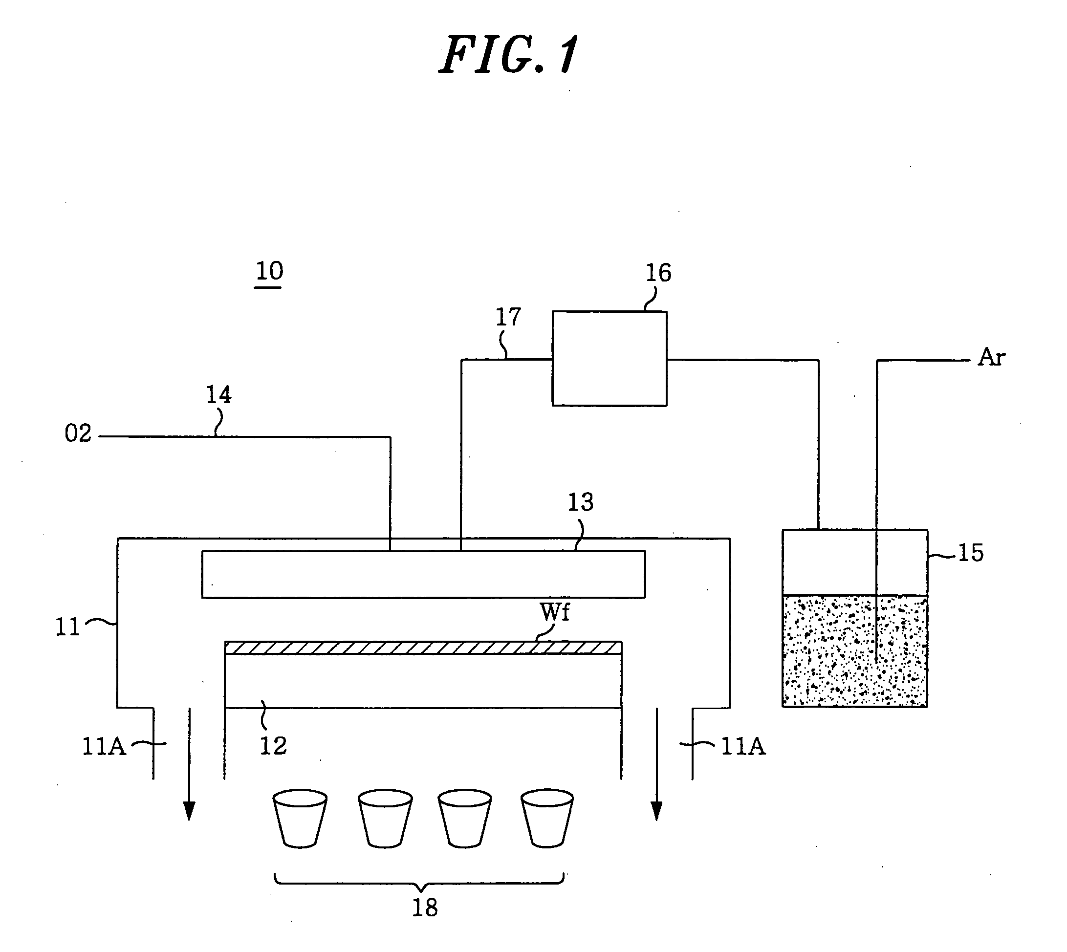
[0026]FIG. 1 shows the structure of a MOCVD film forming apparatus 10 used in a first preferred embodiment of the present invention.

[0027] Referring to FIG. 1, a processing vessel 11 is provided in the MOCVD apparatus 10 at a gas exhaust port 11A to be exhausted by a pump (which is not shown in the drawing); and a substrate supporting table 12 for accommodating a substrate Wf is provided in the processing vessel 11.

[0028] In the MOCVD apparatus 10 of FIG. 1, a showerhead 13 made of aluminum or the like is provided to face the substrate Wf held on the supporting table 12 in the processing vessel 11. A line 14 for feeding oxygen gas into the processing vessel 11 is connected to the showerhead 13. The showerhead 13 is also provided with a source supply system, held in a bubbler 15, for feeding a liquid metal organic compound, e.g., tetra(tert-butoxy)hafnium or the like, into the processing vessel 11 via a controller 16 and a line 17.

[0029] Further, a hea...


PUM

PropertyMeasurementUnit
Temperatureaaaaaaaaaa
Timeaaaaaaaaaa

Abstract

A method of forming a dielectric film by an organic metal CVD method, comprising the step of supplying an organic metal compound into a treating container having a substrate to be treated held therein to form the dielectric film on the substrate, wherein the dielectric film forming step comprises the first step of depositing, in the treating container, the dielectric film under a first condition so set as to allow the residence time of the organic metal compound to extend to a first value, and the second step of further depositing, after the first step and in the treating container, the dielectric film under a second condition so set as to allow the residence time of the organic metal compound to extend to a second value smaller than the first value.

Description

FIELD OF THE INVENTION [0001] The present invention relates to a film forming method; and, more particularly, to a method for forming a dielectric film wherein the dielectric film is formed on a substrate by using a gaseous source material. BACKGROUND OF THE INVENTION [0002] A CVD technique is a film forming method that is widely employed in the process of manufacturing a semiconductor device. [0003] In today's ultrahigh speed semiconductor devices, a gate length can be as short as 0.1 μm or less thanks to the advancement in the miniaturization technique. Generally, the operational speed of a semiconductor device improves with the miniaturization. However, the film thickness of a gate insulating film needs to be reduced in accordance with a scaling rule in such an extremely miniaturized semiconductor device because miniaturization inevitably requires a reduction in the gate length. [0004] Similarly, the film thickness of a capacitor insulating film needs to be decreased to a few nan...

Claims


Application Information

Patent Timeline
IPC IPC(8): H01L21/8238H01L21/31C23C16/40H01L27/04H01L21/28H01L21/316H01L21/822H01L21/8242H01L21/8246H01L27/105H01L27/108H01L29/51H01L29/78
CPCC23C16/405H01L21/28194H01L21/28202H01L29/517H01L27/10852H01L29/513H01L21/31604H01L21/02271H01L21/02189H01L21/022H01L21/02181H10B12/033
Inventor TAKAHASHI, TSUYOSHISHINRIKI, HIROSHIKUBO, KAZUMI
Owner TOKYO ELECTRON LTD
Why Eureka
Try Eureka