Step-down circuit
a step-down circuit and step-down technology, applied in pulse generators, pulse techniques, instruments, etc., can solve the problems of operation failure and increased electric power consumption, and achieve the effects of preventing operation failure, low electric power consumption, and preventing electric power consumption
- Summary
- Abstract
- Description
- Claims
- Application Information
AI Technical Summary
Benefits of technology
Problems solved by technology
Method used
Image
Examples
first embodiment
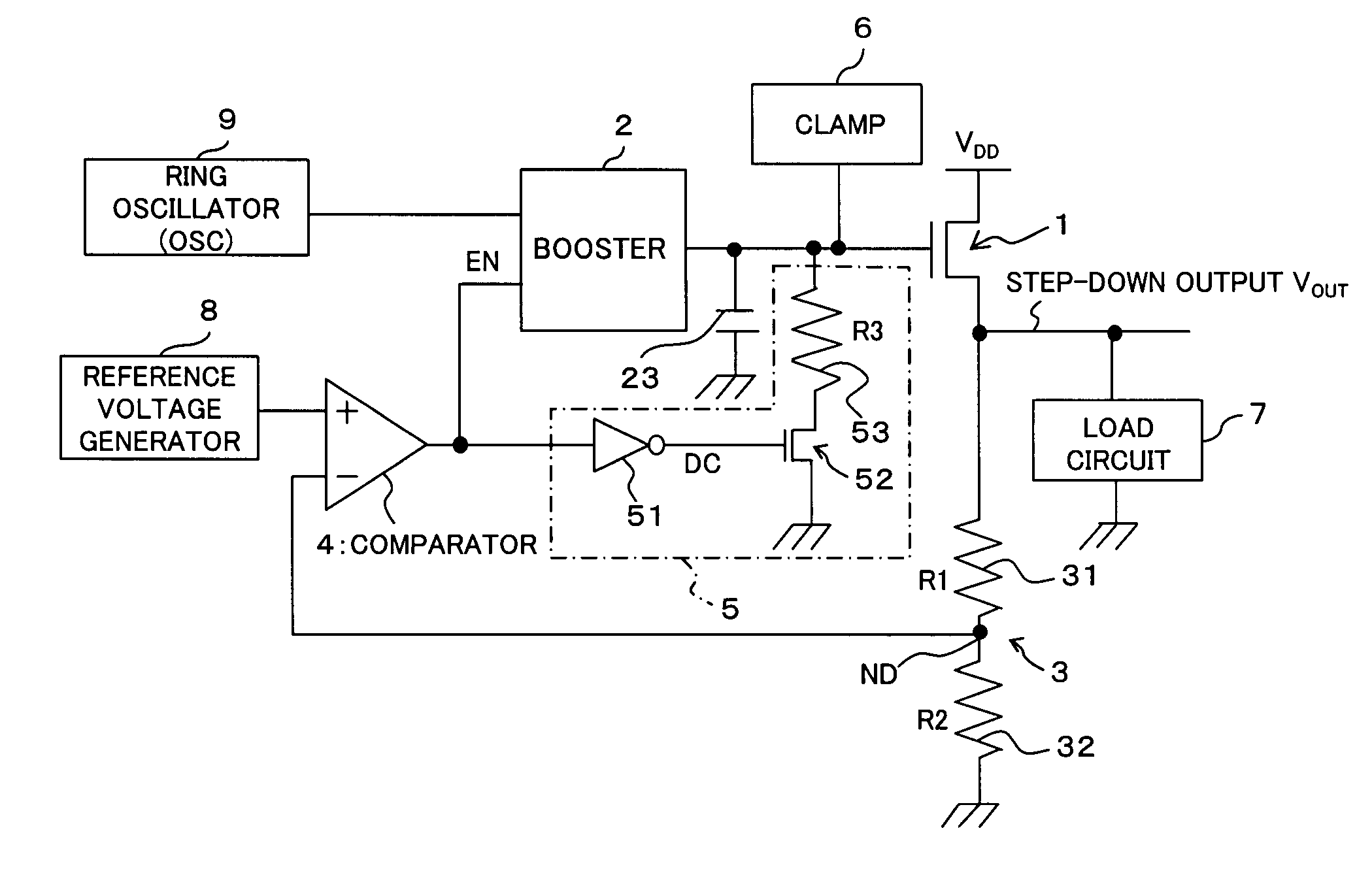
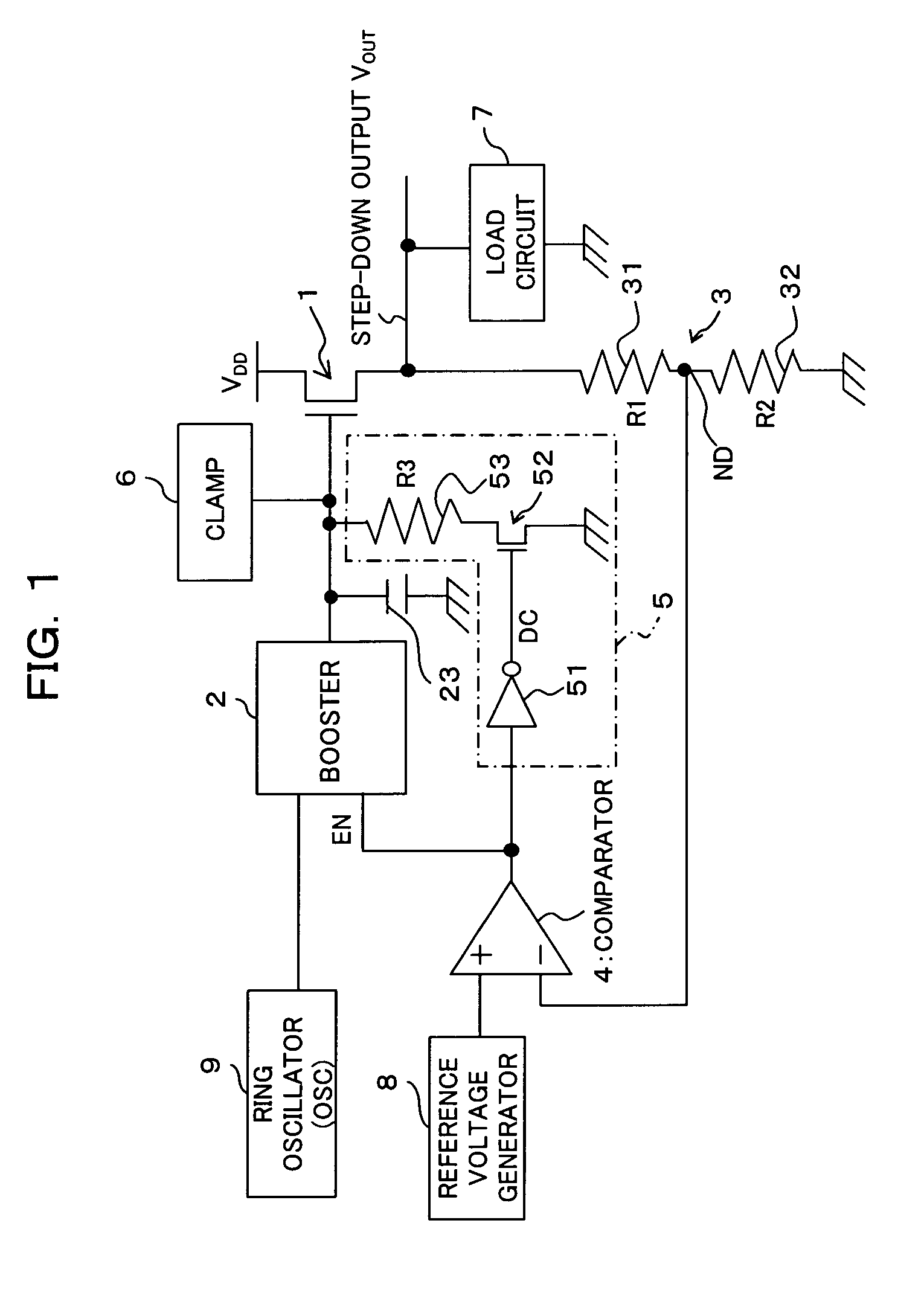
[0036] First of all, referring to FIG. 1 and FIG. 3, the configuration of a step-down circuit according to a first embodiment of the present invention will be described. The step-down circuit according to the embodiment is mounted on, for example, a semiconductor integrated circuit, which steps inputted power supply voltage down to a predetermined step-down voltage to output it to a load circuit. As shown in FIG. 1, the step-down circuit comprises an N channel type (Nch) transistor (output transistor; for example, nMOSFET) 1, a booster 2, a voltage dividing circuit 3 including two resistors 31 and 32 with resistance value R1 and R2 respectively, a comparator 4, a discharge circuit and a clamp circuit 6.
[0037] In this embodiment, taking the stability into consideration, as for the output transistors, not a P channel type transistor but an N channel type transistor is employed.
[0038] Here, a drain (input end) of the output transistor 1 is connected to the power supply line of the po...
second embodiment
[0073] Next, the configuration of a step-down circuit according to a second embodiment of the present invention will be described with reference to FIG. 4 and FIG. 6.
[0074] Compared to the above-described first embodiment, the step-down circuit according to the second embodiment is different in the following points; i.e., the discharge transistor is a P channel type (Pch) transistor, and a level converter is connected to the gate of the P channel type transistor.
[0075] That is, the second embodiment is configured such that, as shown in FIG. 4, the N channel type transistor as the discharge transistor in the above-described first embodiment is replaced with a P channel type transistor (switching transistor; for example, pMOSFET) 60; and the inverter is replace with a level converter [H (High) level converter]61. In FIG. 4, the same elements as those in the above-described first embodiment will be given with the same reference numerals.
[0076] As described-above, the ON resistance o...
third embodiment
[0094] Next, referring to FIG. 7, the configuration of a step-down circuit according to a third embodiment of the present invention will be described.
[0095] Compared to the above-described second embodiment, the step-down circuit according to the third embodiment is different therefrom in the following point. That is, the EN signal, which controls the booster 2 to operate / stop, is fixed to “H” (H level; power supply voltage VDD) to allow the booster 2 to operate anytime. That is, in this embodiment, the input end of the booster 2 for inputting the EN signal is not connected to the output end of the comparator 4, but connected to the power supply line of the power supply voltage VDD so that the EN signal is at “H” (H level; power supply voltage VDD) anytime and the booster 2 is in operation anytime.
[0096] In this case, the booster 2 is allowed to operate anytime, and the step-down voltage (step-down output) VOUT, which is outputted from the output transistor 1, is controlled depend...
PUM
 Abstract
Description
Claims
Application Information


