Nonvolatile semiconductor memory device

a semiconductor memory and non-volatile technology, applied in semiconductor devices, digital storage, instruments, etc., can solve the problems of reducing the reliability of data to be output, unfavorable conventional flash memory, and unfavorable block-by-block basis in view of energy saving, so as to minimize the effect of time consumption on the erasing action

Inactive Publication Date: 2006-01-19
SHARP KK
View PDF5 Cites 18 Cited by
  • Summary
  • Abstract
  • Description
  • Claims
  • Application Information

AI Technical Summary

Benefits of technology

[0031] As featured, the not erased sectors determined after the verifying process can selectively be accessed and subjected to the second and further erasing actions, whereby the overall erasing action will be minimized in the time consumption.

Problems solved by technology

Such a conventional flash memory is however unfavorable in the erasing property of the memory cell array.
As a result, the data to be output will be lowered in the reliability.
Moreover, the block-by-block basis may be unfavorable in view of the energy saving.
Those requirements will disadvantageously increase the current consumption and the overall chip area.
Also, with the fact that the charge pump circuit in a common flash memory delivers 1 mA of current at minimum, the total current of 50 mA for collective erasing will rarely be feasible.

Method used


Image

  • Nonvolatile semiconductor memory device
  • Nonvolatile semiconductor memory device
  • Nonvolatile semiconductor memory device

Examples


Embodiment Construction

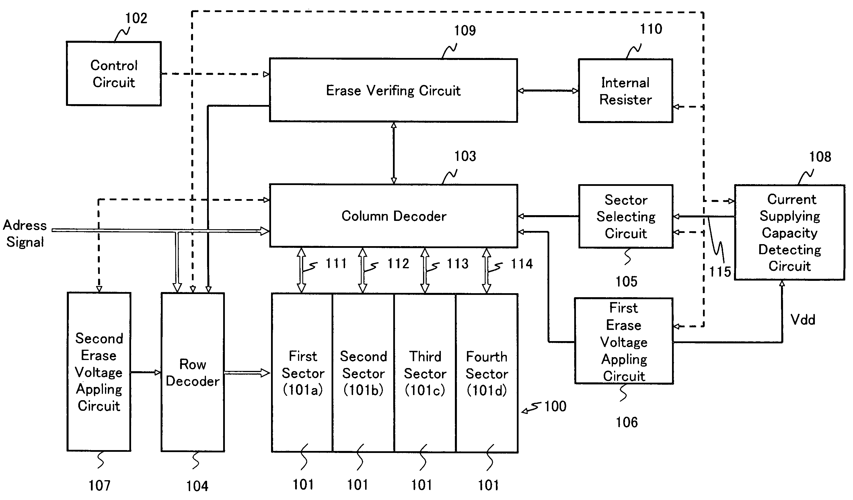
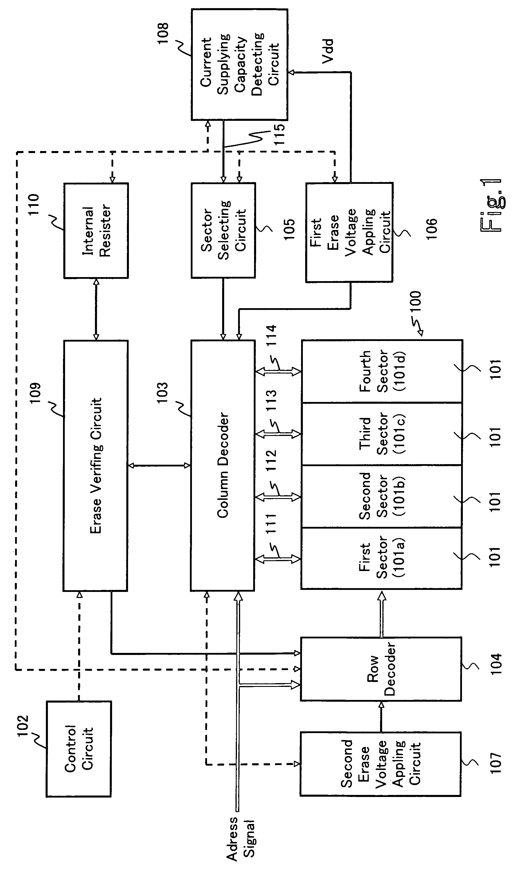
[0041] One embodiment of the present invention will be described in the form of a nonvolatile semiconductor memory device (referred to as an inventive device hereinafter), referring to relevant drawings.

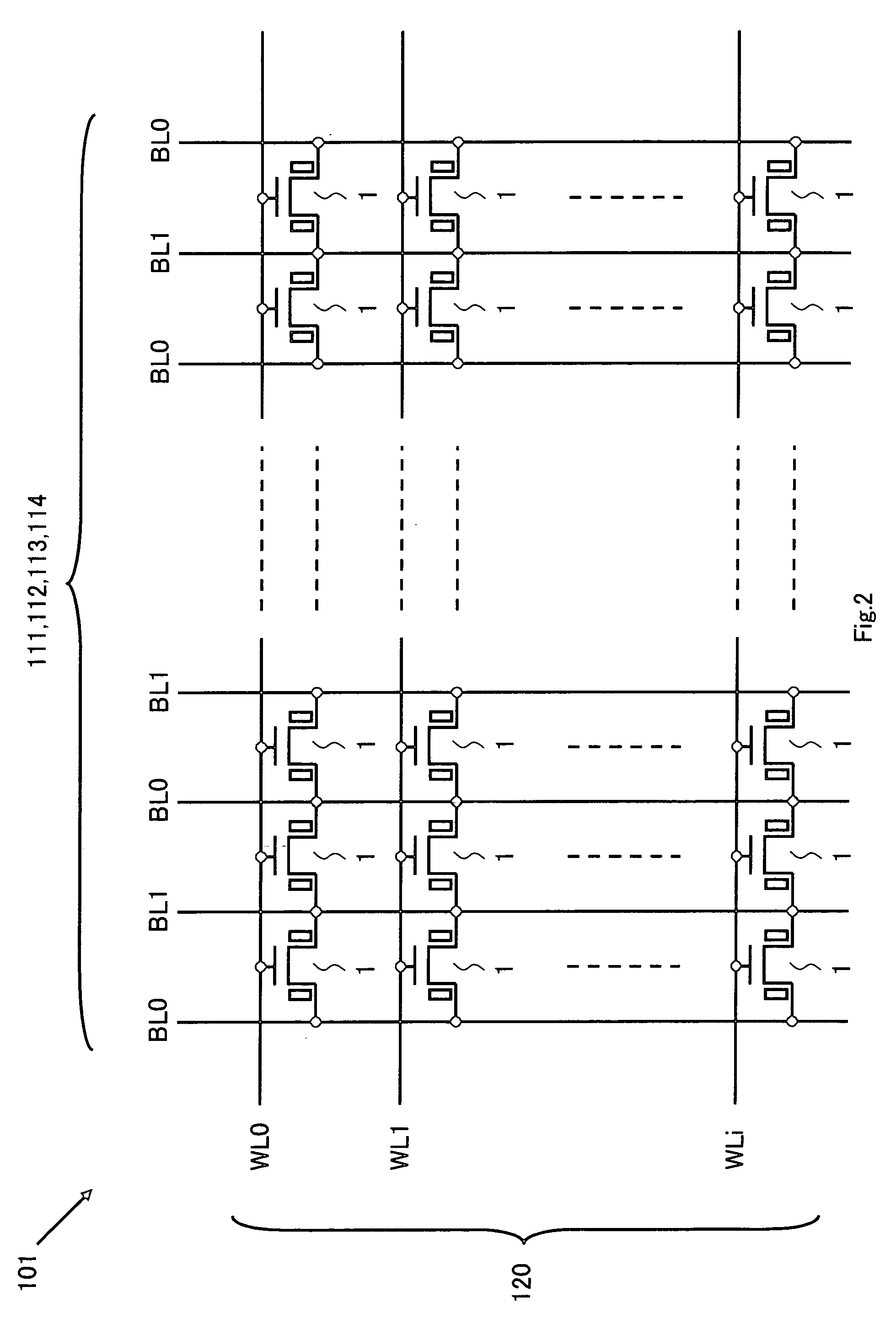
[0042]FIG. 1 is a schematic block diagram of the inventive device. Shown in FIG. 1 is a circuit block of the inventive device for conducting an erasing action. The inventive device comprises a group of memory cell arrays 100, each array consisting mainly of sidewall type memory cells (referred to as memory cells hereinafter) arrayed in a matrix form having rows and columns. FIG. 1 illustrates one memory cell array 100 for simplification. The memory cell array 100 is divided into a plurality of sectors 101. Four of the sectors 101 separated uniformly along a column are shown in FIG. 1 while the sectors in each memory cell array 101 are not limited to the number and the direction of division in the embodiment. As the memory cell array 100 in the inventive device is selected with an er...


PUM


Abstract

A nonvolatile semiconductor memory device is provided comprising a plurality of memory cell arrays, each of which consists mainly of sidewall type memory cells arranged in a matrix, the memory cell having a MOSFET structure where memory functional element for holding charges are provided on both sides of a gate electrode. The memory cell array is divided into sectors. The memory device further comprises a sector selecting circuit for, when one of the memory cell arrays is to be erased collectively, sequentially selecting at most a predetermined number of the sectors at a time from the memory cell array to be erased, and an erase voltage applying circuit for, when the collective erasing action is carried out, applying a predetermined level of erasing voltage to the sectors selected at once by the sector selecting circuit.

Description

CROSS REFERENCE TO RELATED APPLICATION [0001] This Nonprovisional application claims priority under 35 U.S.C. §119(a) on Patent Application No. 2004-209353 filed in Japan on Jul. 16, 2004, the entire contents of which are hereby incorporated by reference. BACKGROUND OF THE INVENTION [0002] 1. Field of the Invention [0003] The present invention relates to a nonvolatile semiconductor memory device which comprises one or more memory cell arrays erasable collectively in response to a command input from the outside, each memory cell array having a plurality of a sidewall type memory cell arranged in a matrix form of rows and columns and each sidewall type memory cell comprising a gate electrode formed over a semiconductor layer via a gate insulating film, a channel region disposed below the gate electrode, diffusion regions disposed on both sides of the channel region and having a conductive type opposite to that of the channel region, and a memory functional element formed on either bot...

Claims


Application Information

Patent Timeline
Patent Type & Authority Applications(United States)
IPC IPC(8): G11C16/06
CPCG11C16/0475G11C16/0491H01L29/7923G11C16/344H01L27/115G11C16/16H10B69/00
Inventor MATSUOKA, NOBUAKI
Owner SHARP KK
Why Eureka
Try Eureka