Magnetic tunnel junction element structures and methods for fabricating the same

a technology of element structure and tunnel junction, which is applied in the manufacture of inductance/transformer/magnet, magnetic bodies, instruments, etc., can solve the problems of reducing reliability and thus process yield in mtj device fabrication

Active Publication Date: 2006-01-26
HEADWAY TECH INC
View PDF13 Cites 110 Cited by
  • Summary
  • Abstract
  • Description
  • Claims
  • Application Information

AI Technical Summary

Problems solved by technology

Typically, surface roughness of the tunnel barrier leads to a reduction of MR due to non-tunnel current flow through the barrier or over oxida

Method used


Image

  • Magnetic tunnel junction element structures and methods for fabricating the same
  • Magnetic tunnel junction element structures and methods for fabricating the same
  • Magnetic tunnel junction element structures and methods for fabricating the same

Examples


Embodiment Construction

[0011] The following detailed description of the invention is merely exemplary in nature and is not intended to limit the invention or the application and uses of the invention. Furthermore, there is no intention to be bound by any theory presented in the preceding background of the invention or the following detailed description of the invention.

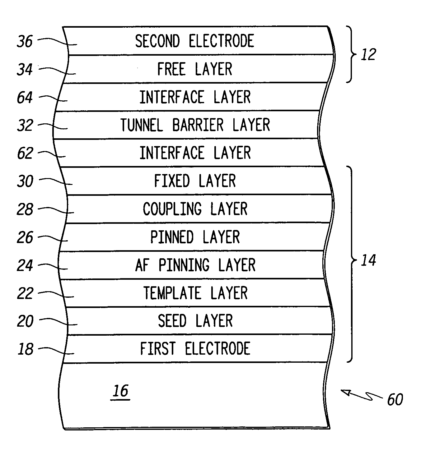
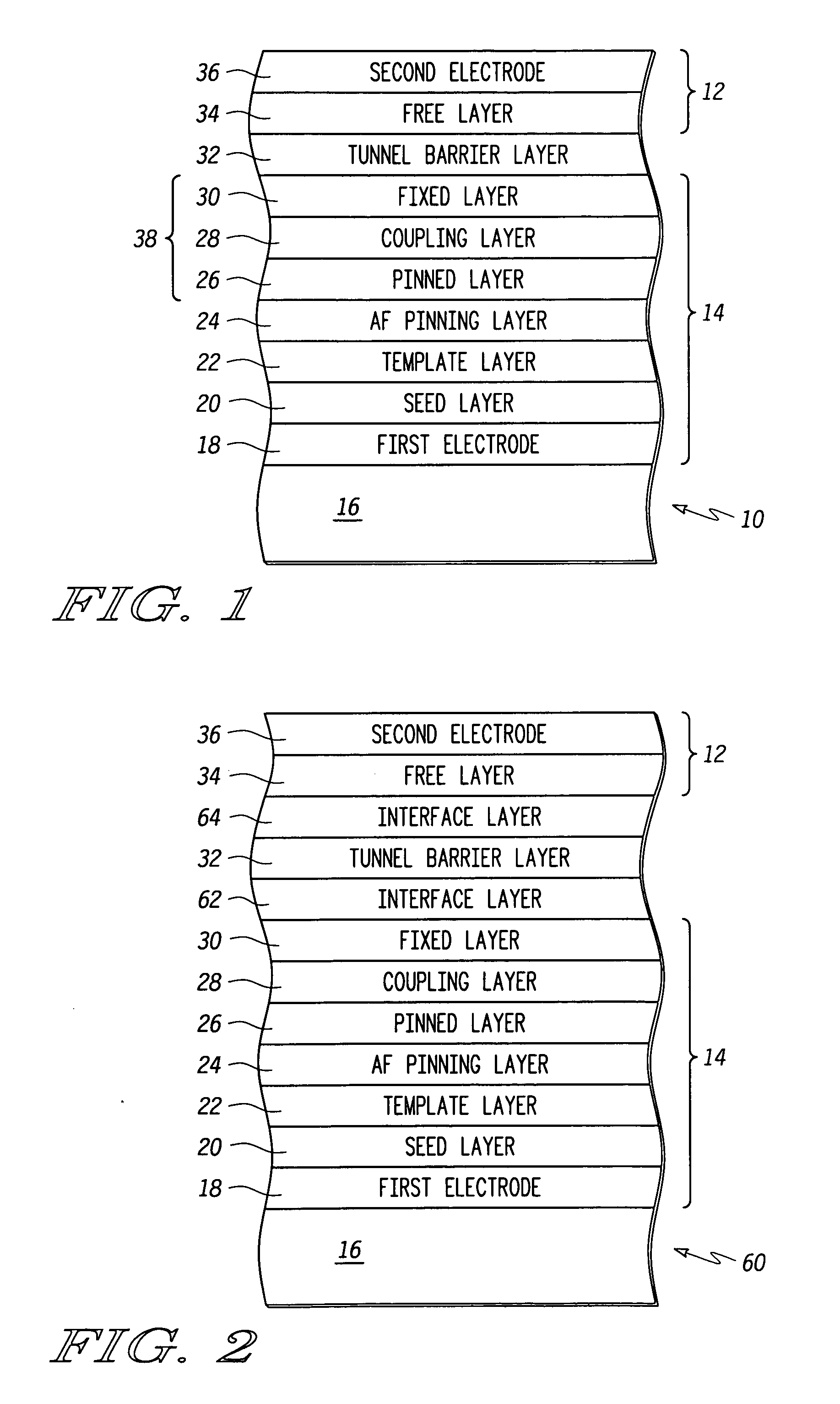
[0012] Referring to FIG. 1, an MTJ element 10 in accordance with one exemplary embodiment of the present invention comprises a substrate 16, a first electrode multilayer stack 14, a second electrode multilayer stack 12, and an insulating tunnel barrier layer 32 disposed between the first electrode multilayer stack 14 and the second electrode multilayer stack 12. Substrate 16 may comprise any suitable insulating material, such as, for example, a dielectric material. First electrode multilayer stack 14 and second electrode multilayer stack 12 include ferromagnetic layers, as described in more detail below. Tunnel barrier layer 32 preferably ...


PUM


Abstract

Magnetic tunnel junction (“MTJ”) element structures and methods for fabricating MTJ element structures are provided. An MTJ element structure may comprise a crystalline pinned layer, an amorphous fixed layer, and a coupling layer disposed between the crystalline pinned layer and the amorphous fixed layer. The amorphous fixed layer is antiferromagnetically coupled to the crystalline pinned layer. The MTJ element further comprises a free layer and a tunnel barrier layer disposed between the amorphous fixed layer and the free layer. Another MTJ element structure may comprise a pinned layer, a fixed layer and a non-magnetic coupling layer disposed therebetween. A tunnel barrier layer is disposed between the fixed layer and a free layer. An interface layer is disposed adjacent the tunnel barrier layer and a layer of amorphous material. The first interface layer comprises a material having a spin polarization that is higher than that of the amorphous material.

Description

FIELD OF THE INVENTION [0001] The present invention relates generally to magnetoelectronic devices, and more particularly relates to magnetic tunnel junction element structures and methods for fabricating magnetic tunnel junction element structures. BACKGROUND OF THE INVENTION [0002] Magnetoelectronics devices, spin electronics devices, and spintronics devices are synonymous terms for devices that use the effects predominantly caused by electron spin. Magnetoelectronics effects are used in numerous information devices, and provide non-volatile, reliable, radiation resistant, and high-density data storage and retrieval. The numerous magnetoelectronics information devices include, but are not limited to, magnetic random access memory (MRAM), magnetic sensors, and read / write heads for disk drives. [0003] Typically, a magnetoelectronic device, such as a magnetic memory element, has a structure that includes multiple ferromagnetic layers separated by at least one non-magnetic layer. In t...

Claims


Application Information

Patent Timeline
IPC IPC(8): H01L29/94
CPCB82Y25/00B82Y40/00H01F10/132H01L43/12H01F10/3272H01F41/303H01L43/08H01F10/3254H10N50/10H10N50/01G11C11/15
Inventor SUN, JIJUNDAVE, RENU W.SLAUGHTER, JON M.AKERMAN, JOHAN
Owner HEADWAY TECH INC
Why Eureka
Try Eureka