Light-emitting device and method of manufacturing the same

a technology of light-emitting devices and manufacturing methods, which is applied in the direction of sustainable manufacturing/processing, instruments, and final product manufacturing, etc., can solve the problems of deterioration of organic el films

Inactive Publication Date: 2006-01-26
SEMICON ENERGY LAB CO LTD
View PDF42 Cites 40 Cited by
  • Summary
  • Abstract
  • Description
  • Claims
  • Application Information

AI Technical Summary

Benefits of technology

[0009] The present invention has been made in order to solve the above problem, and therefore has an object to provide a bright and highly reliable light-emitting device. Further, another object of the present invention is to provide highly reliable electric equipment that uses the light-emitting device as its display portion or light source.
[0018] An effect of the present invention is in that the extraction of the emission of light of the EL light-emitting device from the side of the cathode, which in the prior art had been difficult, can now be carried out with ease. This effect is particularly remarkable during the formation of the active matrix type EL light-emitting device.

Problems solved by technology

Therefore, the necessity of raising the luminance of the light emitted in order to obtain a bright image leads to the result of hastening the deterioration of the organic EL film.

Method used


Image

  • Light-emitting device and method of manufacturing the same
  • Light-emitting device and method of manufacturing the same
  • Light-emitting device and method of manufacturing the same

Examples


embodiment 1

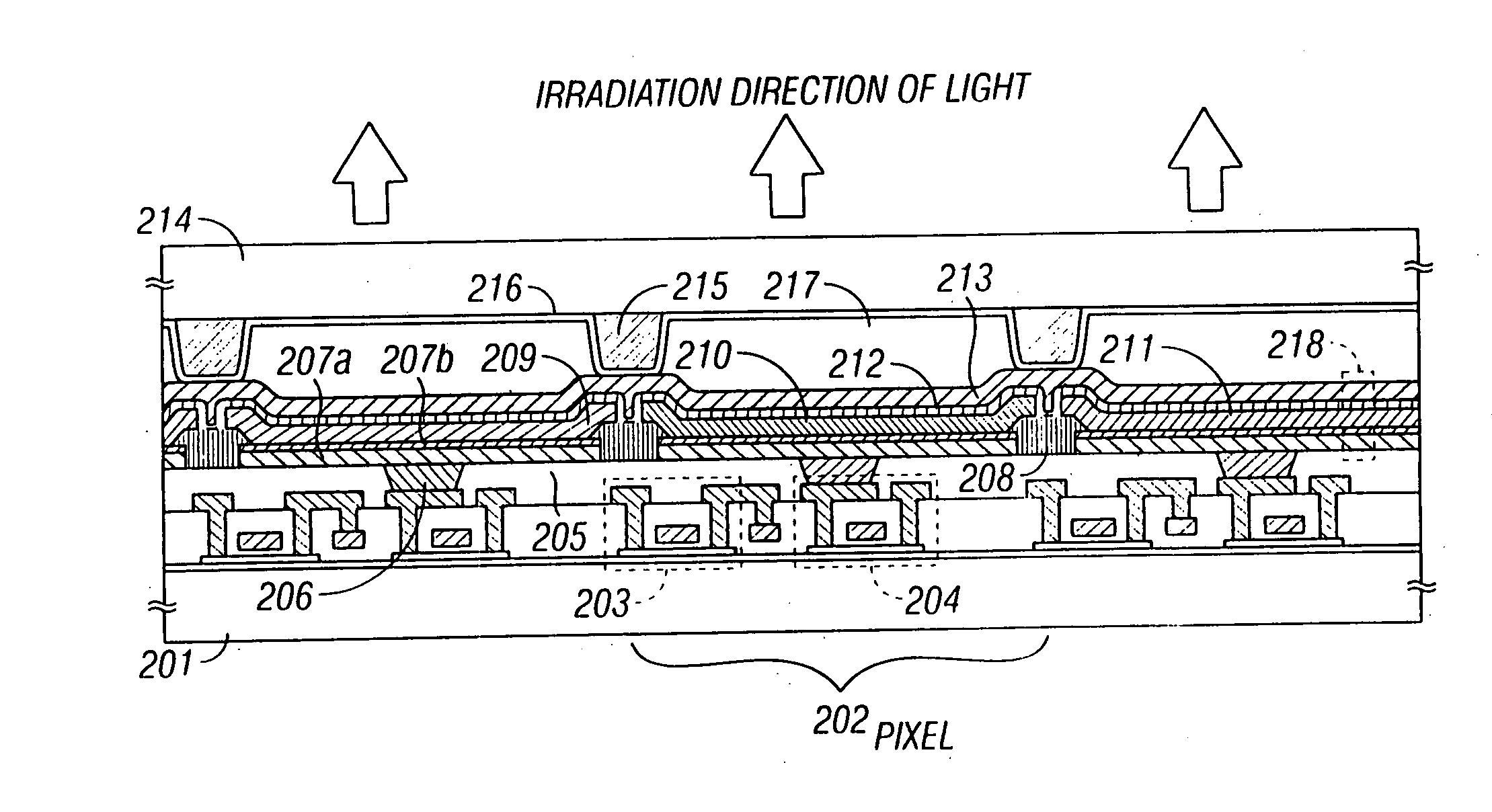
[0043] Embodiment 1 will be explained with reference to FIGS. 3A to 5B. Note that shown in FIGS. 3A to 4D are cross sectional views of manufacturing processes in a pixel portion. Furthermore, the top view of a pixel formed in accordance with Embodiment 1 (a top view at the point of the formation of an anode) is shown in FIG. 5A, and a final circuit configuration of the pixel is shown in FIG. 5B. It is to be noted that the reference numerals used in FIGS. 5A and 5B correspond to those used in FIGS. 3A to 4D.

[0044] First, as shown in FIG. 3A, a glass substrate 301 is prepared as the element-forming substrate, and an insulating film 302 made of a silicon oxide film is formed thereon to a thickness of 200 nm. The insulating film 302 may be formed by employing low pressure thermal CVD, plasma CVD, sputtering, or evaporation.

[0045] A crystalline silicon film 303 is next formed to a thickness of 50 nm on the insulating film 302. A known method may be used as the formation method of the c...

embodiment 2

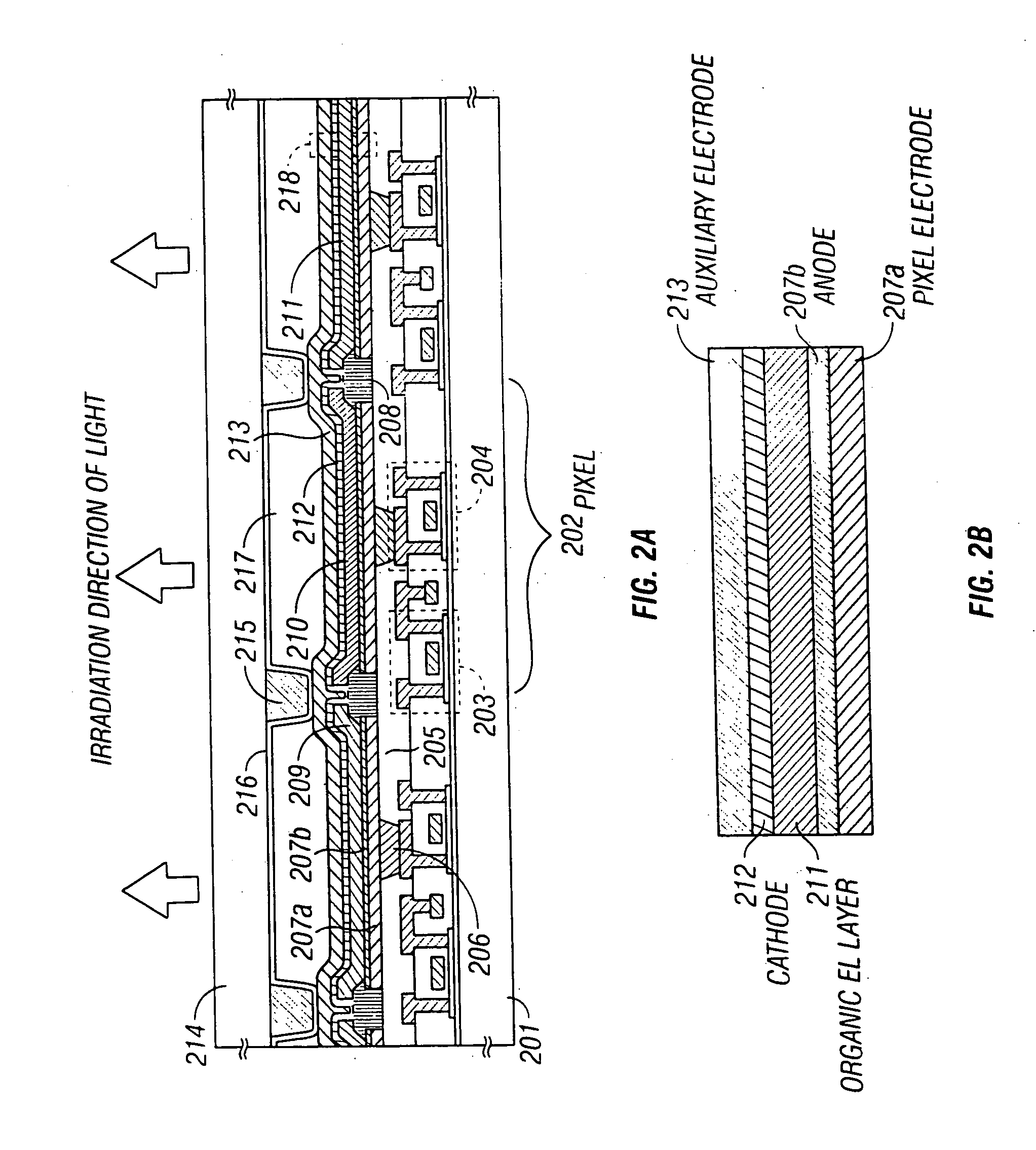
[0076] In Embodiment 2, an explanation will be made with reference to FIG. 6 on an EL light-emitting device having a pixel with a structure that is different from that of the EL light-emitting device shown in FIG. 2. Note that in Embodiment 2, the structure of the EL light-emitting device may be manufactured by adding a few changes to the structure of FIG. 2, and hence explanations will be made on the points that are different from those of FIG. 2. Therefore, the embodiment mode may be referenced concerning the explanation of the parts that are denoted by the same reference numerals with those of FIG. 2.

[0077] In Embodiment 2, upon forming a contact hole in the interlayer insulating film 205, a pixel electrode 601a and an anode 601b are formed in this state. Then, an insulating film 602 is formed to fill up the concave portion formed by the contact hole. The insulating film 602 is called a filling-up insulating film in Embodiment 2. The filling-up insulating film 602 can be formed ...

embodiment 3

[0083] Although only the structure of the pixel portion is shown in the EL light-emitting device illustrated in Embodiment 1, a driver circuit for driving the pixel portion may be formed integrally therewith on the same substrate. When forming the driver circuit, the driver circuit may be formed of an nMOS circuit, a pMOS circuit, or a CMOS circuit. Of course, only the pixel portion may be formed of a TFT, and a driver circuit containing an IC chip may be used as an external-attached driver circuit.

[0084] Further, the manufacturing processes in Embodiment 1 are reduced by forming the pixel portion with the P channel TFT only. However, in case of Embodiment 2, the driver circuit is formed of the pMOS circuit, and a driver circuit containing an IC chip can be used as the driver circuit that cannot be formed of the pMOS circuit.

[0085] Note that the constitution of Embodiment 2 may be implemented by freely combining it with the constitution of Embodiment 1 or 2.


PUM


Abstract

To provide a bright and highly reliable light-emitting device. An anode (102), an EL layer (103), a cathode (104), and an auxiliary electrode (105) are formed sequentially in lamination on a reflecting electrode (101). Further, the anode (102), the cathode (104), and the auxiliary electrode (105) are either transparent or semi-transparent with respect to visible radiation. In such a structure, lights generated in the EL layer (103) are almost all irradiated to the side of the cathode (104), whereby an effect light emitting area of a pixel is drastically enhanced.

Description

CROSS-REFERENCE TO RELATED APPLICATIONS [0001] This application is a continuation application of U.S. application Ser. No. 10 / 896,028, filed Jul. 22, 2004, which is a continuation of U.S. application Ser. No. 10 / 370,739, filed Feb. 24, 2003, now U.S. Pat. No. 6,768,260, which is a divisional of U.S. application Ser. No. 09 / 774,653, filed Feb. 1, 2001, now U.S. Pat. No. 6,559,594, which claims the benefit of a foreign priority application filed in Japan as Ser. No. 2000-026879 on Feb. 3, 2000. This application claims priority to each of these prior applications, and the disclosures of the prior applications are considered part of (and are incorporated by reference in) the disclosure of this application.BACKGROUND OF THE INVENTION [0002] 1. Field of the Invention [0003] The present invention relates to a light-emitting device using a thin film that is made of a luminous material. Further, the present invention relates to electric equipment using the light-emitting device as a display ...

Claims


Application Information

Patent Timeline
Patent Type & Authority Applications(United States)
IPC IPC(8): H01J1/62H01L21/77H01L27/12H05B33/26H01L27/32H01L29/786H01L51/52H01L51/56
CPCH01L27/12H01L51/0097H01L27/3211H01L27/3244H01L27/3246H01L27/3248H01L27/3262H01L27/3295H01L29/78645H01L29/78669H01L51/5206H01L51/5218H01L51/5228H01L51/5234H01L51/5237H01L51/525H01L51/5271H01L51/56H01L2251/5315H01L27/15Y10S428/917H01L27/1288H01L27/3276H01L27/1214Y02E10/549Y02P70/50H10K59/35H10K59/123H10K59/122H10K59/12H10K59/1213H10K50/818H10K50/824H10K50/828H10K50/8428H10K50/856H10K2102/3026H10K71/00G07F9/105G07F13/065H10K50/81H10K59/131H10K77/111H10K50/84
Inventor FUKUNAGA, TAKESHIMARUYAMA, JUNYA
Owner SEMICON ENERGY LAB CO LTD
Why Eureka
Try Eureka