Electro-optical device, electronic apparatus, and mounting structure

Active Publication Date: 2006-01-26
BOE TECH GRP CO LTD
View PDF5 Cites 4 Cited by
  • Summary
  • Abstract
  • Description
  • Claims
  • Application Information

AI Technical Summary

Benefits of technology

[0008] An advantage of the invention is that it provides an electro-optical device, an electronic apparatus having the electro-optical device, and a mounting structure capable of easily diagnosing a connection state between terminals at a mounting portions when an IC is mounted on a substrate directly or through a wiring substrate.
[0009] Another advantage of the invention is that it provides an electro-optical device, an electronic apparatus having the electro-optical device, and a mounting structure capable of easily detecting whether a defect occurs in an IC or a substrate and of outputting the detected result.
[0010] According to a first aspect of the invention, there is provided an electro-optical device including a first substrate that holds an electro-optical material, a first IC that is mounted on the first substrate and that has a plurality of first terminals, a plurality of second terminals that are formed on the first substrate to be connect to the plurality of first terminals, a plurality of wiring lines formed on the first substrate, first connection state diagnostic terminals that are included in the plurality of first terminals and that are used for diagnosing connection states between the first terminals and the second terminals, second connection state diagnostic terminals that are included in the plurality of second terminals and that are connected to the first connection state diagnostic terminals, respectively, a connection state diagnostic unit that is provided in the first IC to diagnose whether the first and second connection state diagnostic terminals are electrically connected to each other, and a connection state diagnosis result output unit that is provided in the first IC and that outputs a diagnosis result obtained by the connection state diagnostic unit.
[0011] According to the first aspect of the invention, the first connection state diagnostic terminals are included in the plurality of first terminals of the first IC, and the second connection state diagnostic terminals connected to the first connection state diagnostic terminals are included in the plurality of second terminals of the first substrate. For this reason, in a state in which the first IC is mounted on the first substrate, the connection state diagnostic unit determines that good connection is obtained between the second connection state diagnostic terminals and the first connection state diagnostic terminals when the second connection state diagnostic terminals and the first connection state diagnostic terminals are electrically connected to each other, and determines that poor connection is obtained between the second connection state diagnostic terminals and the first connection state diagnostic terminals when the second connection state diagnostic terminals and the first connection state diagnostic terminals are not electrically connected to each other. After that, the diagnosis results are output by the connection state diagnosis result output unit. Therefore

Problems solved by technology

However, when a defect occurs in any one of these ICs, a great deal of labor is required to pinpoint the cause of the defect.
In the electro-optical device disclosed in Japanese Unexamined Patent Application Publication No. 2003-57677, when a defect occurs in mounting an IC on a substrate and poor connection is obtained between terminals of the IC and terminals of the substrate, a display defect occurs.
However, it is difficult to find such a connection defect even tho

Method used


Image

  • Electro-optical device, electronic apparatus, and mounting structure
  • Electro-optical device, electronic apparatus, and mounting structure
  • Electro-optical device, electronic apparatus, and mounting structure

Examples


Example

First Embodiment

Overall Structure of Electro-Optical Device

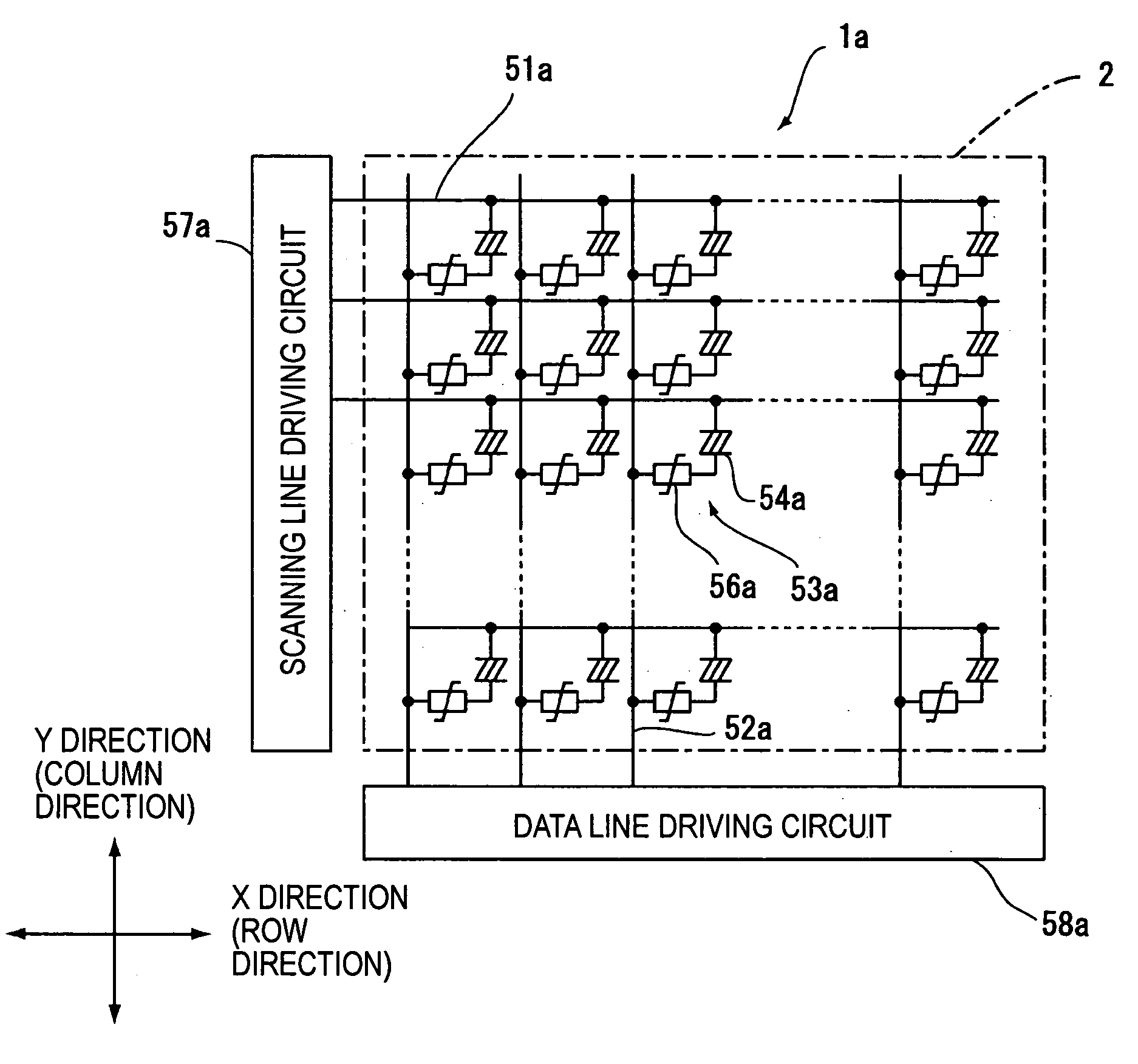
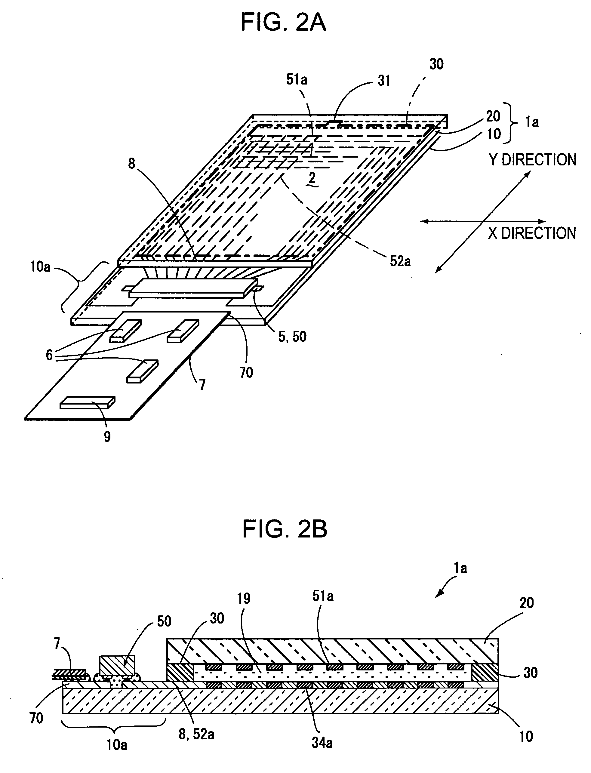
[0037]FIG. 1 is a block diagram illustrating the electrical structure of an electro-optical device. FIG. 2A is a schematic perspective view illustrating an electro-optical device according to an embodiment of the invention, as viewed from a counter substrate, and FIG. 2B is a cross-sectional view taken along the Y direction of the electro-optical device to pass through pixel electrodes.

[0038] An electro-optical device 1a shown in FIG. 1 is an active matrix liquid crystal device using thin film diodes (TFDs) as pixel switching elements. In an image display region 2 of the electro-optical device 1a, when two directions orthogonal to each other are the X direction and the Y direction, a plurality of scanning lines 51a extends in the X direction (row direction), and a plurality of data lines 52a extends in the Y direction (column direction). Also, in the image display region 2 of the electro-optical device 1a, a plurality of...

Example

Second Embodiment

[0061]FIG. 5 is an explanatory diagram illustrating a self-diagnostic structure among various components of an electro-optical device according to a second embodiment of the invention. Since the electro-optical device of the second embodiment has the same basic structure as that in the first embodiment, components having the same functions as those in the first embodiment have the same reference numerals, and thus the description thereof will be omitted.

[0062] In the electro-optical device 1a shown in FIG. 5, as described in the first embodiment, the element substrate 10, which is the first substrate, and the counter substrate 20, which is the second substrate, are bonded to each other with an intersubstrate conductive material interposed therebetween, so that the intersubstrate connecting terminals are electrically connected to each other. In the present embodiment, of the element substrate 10 and the counter substrate 20, the driving IC 5 and the flexible substr...

Example

Third Embodiment

[0068]FIG. 6 is an explanatory diagram illustrating a self-diagnostic structure among various components of an electro-optical device according to a third embodiment of the invention. In the first and second embodiments, the driving IC 5 is mounted on the element substrate 10 in a COG manner. However, in the present embodiment, the driving IC 5 is mounted on the flexible substrate 7 in a COF manner. Here, since the electro-optical device of the third embodiment has the same basic structure as that in the first embodiment, components having the same functions as those in the first embodiment have the same reference numerals, and thus the description thereof will be omitted.

[0069] As shown in FIG. 6, in the electro-optical device 1a of the present embodiment, the element substrate 10 is mounted with the flexible substrate 7 (the wiring substrate) having the driving IC 5 (the first IC), the auxiliary ICs 6 (the second ICs), and the connector 9 thereon. Therefore, a pl...


PUM


Abstract

An electro-optical device includes a first substrate that holds an electro-optical material, a first IC that is mounted on the first substrate and that has a plurality of first terminals, a plurality of second terminals that are formed on the first substrate to be connected to the plurality of first terminals, respectively, a plurality of wiring lines formed on the first substrate, first connection state diagnostic terminals that are included in the plurality of first terminals and that are used for diagnosing connection states between the first terminals and the second terminals, second connection state diagnostic terminals that are included in the plurality of second terminals and that are connected to the first connection state diagnostic terminals, respectively, a connection state diagnostic unit that is provided in the first IC to diagnose whether the first and second connection state diagnostic terminals are electrically connected to each other, and a connection state diagnosis result output unit that is provided in the first IC and that outputs a diagnosis result obtained by the connection state diagnostic unit.

Description

BACKGROUND OF THE INVENTION [0001] 1. Technical Field [0002] The present invention relates to an electro-optical device, an electronic apparatus having the same, and a mounting structure in which a member is mounted on a mounting substrate, and more particularly, to a technique of performing the diagnosis of an electro-optical device and a mounting structure. [0003] 2. Related Art [0004] In general, in electro-optical devices, such as active matrix liquid crystal devices, a driving IC and a flexible substrate are mounted on an electro-optical device substrate holding an electro-optical material, and each pixel is driven by signals output from the driving IC or signals generated based on the signals output from the driving IC (for example, see Japanese Unexamined Patent Application Publication No. 2003-57677). [0005] Further, an electro-optical device substrate or a flexible substrate has a power supply IC, an EPROM, an IC for driving an LED for a backlight, etc. mounted thereon, in ...

Claims


Application Information

Patent Timeline
IPC IPC(8): G06E3/00
CPCG06E3/005G02F1/1345
Inventor HASEGAWA, KENICHITSUDA, ATSUNARI
Owner BOE TECH GRP CO LTD
Why Eureka
Try Eureka