Method and system for electron density measurement

a technology of electron density and measurement method, applied in the field of plasma processing, can solve the problems of complex diagnostic system employed in semiconductor manufacturing and requires experienced personnel to opera

Inactive Publication Date: 2006-02-16
TOKYO ELECTRON LTD
View PDF4 Cites 6 Cited by
  • Summary
  • Abstract
  • Description
  • Claims
  • Application Information

AI Technical Summary

Benefits of technology

[0006] The present invention relates to a method and system for monitoring electron density during plasma processing. The present invention advantageously provides a method and system that enables semiconductor manufacturers to satisfy more stringent performance requirements for material processing equipment used in the semiconductor industry.

Problems solved by technology

However, the diagnostic system employed in semiconductor manufacturing can be complex and, in general, can require experienced personnel to operate.

Method used


Image

  • Method and system for electron density measurement
  • Method and system for electron density measurement
  • Method and system for electron density measurement

Examples


Embodiment Construction

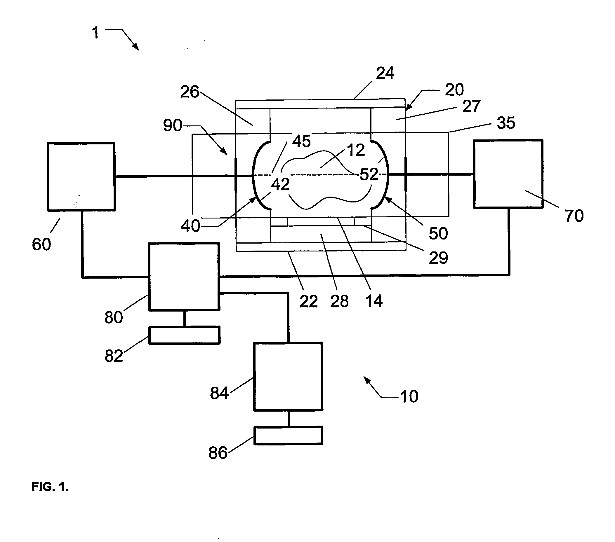
[0033] The present invention generally relates to fabrication of integrated circuits in the semiconductor industry. The present invention advantageously provides a method and apparatus that enables semiconductor manufacturers to satisfy more stringent performance requirements for material processing equipment used in the semiconductor industry.

[0034] A method of improving the performance of material processing equipment is to monitor and control plasma electron density within the processing chamber during the manufacturing process. Ideally, the plasma electron density is maintained such that the processes being performed are uniformly acting upon the entire surface of the substrate upon which a process is being performed.

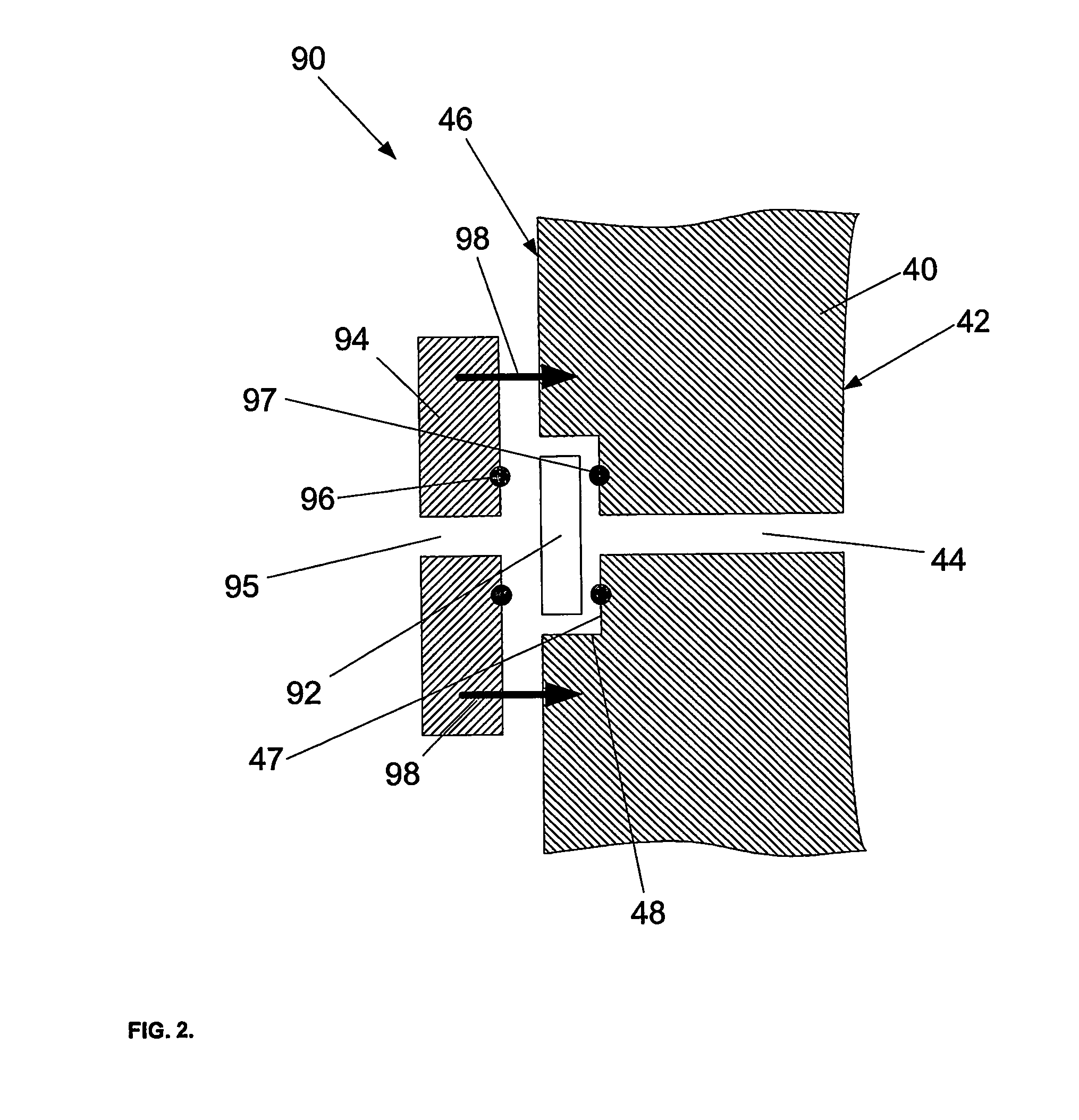
[0035] An exemplary device used to measure plasma electron density is a microwave system of suitably high frequency to exceed the electron plasma frequency. The device includes a pair of mirrors immersed in the plasma. Microwave power is coupled to a first microwa...


PUM

PropertyMeasurementUnit
center frequencyaaaaaaaaaa

Abstract

The present invention provides a diagnostic system for plasma processing, wherein the diagnostic system comprises a multi-modal resonator, a power source, a detector, and a controller. The controller is coupled to the power source and the detector and it is configured to provide a man-machine interface for performing several monitoring and controlling functions associated with the diagnostic system including: a Gunn diode voltage monitor, a Gunn diode current monitor, a varactor diode voltage monitor, a detector voltage monitor, a varactor voltage control, a varactor voltage sweep control, a resonance lock-on control, a graphical user control, and an electron density monitor. The diagnostic system can further provide a remote controller coupled to the controller and configured to provide a remote man-machine interface. The remote man-machine interface. The remote man-machine interface can provide a graphical user interface in order to permit remote control of the diagnostic system by an operator. In addition, the present invention provides several methods of controlling the diagnostic system in order to perform both monitor and control functions.

Description

CROSS-REFERENCE TO RELATED APPLICATIONS [0001] This application is related to co-pending International Application No. PCT / US00 / 19539, Publication No. WO 01 / 06402, published on Jan. 25, 2001; International Application No. PCT / US00 / 19536, Publication No. WO 01 / 06544, published on Jan. 25, 2001; International Application No. PCT / US00 / 19535, Publication No. WO 01 / 06268, published on Jan. 25, 2001; International Application No. PCT / US00 / 19540, filed on Jul. 20, 2001; pending application Ser. No. 60 / 330,518, entitled “Method and apparatus for wall film monitoring”, Attorney docket No. 212961 US6YA PROV, filed on Oct. 24, 2001; pending application Ser. No. 60 / 330,555, entitled “Method and apparatus for electron density measurement”, Attorney docket No. 212759US6YA PROV, filed on Oct. 24, 2001; pending application Ser. No. 60 / 352,502, entitled “Method and apparatus for electron density measurement and verifying process status,” Attorney docket. No. 218217US6YA PROV filed on Jan. 31, 2002; ...

Claims


Application Information

Patent Timeline
Patent Type & Authority Applications(United States)
IPC IPC(8): G01N19/02G01N3/56H01J37/32
CPCH01J37/32192H01J37/3299H01J37/32935
Inventor STRANG, ERIC J.PARSONS, RICHARDGOLDFIELD, JODY
Owner TOKYO ELECTRON LTD
Why Eureka
Try Eureka