
Eureka
For R&D, Eureka makes reading and utilizing patents & technical documents easy.
Eureka AIR
Designed for self-driven R&D workflows. Generate viable solutions, solve complex R&D challenges, empower your innovation with AI.

Eureka Materials
Designed for material experts only. Revolutionize your material R&D, from search, analyze, to developing new materials.

TechResearch
Generate reliable direction feasibility study reports for your R&D in just a few steps.

TechSeek
Discover and master advanced knowledge NOW. Basics, ideas, possibilities, all at once.

TechMind
As an expert in R&D Theories, TechMind can generates customized viable solutions instantly.

TechRisk
Analyze your overall solution with one click, know your potential R&D risks in advance.

TechMonitor
Get weekly tech updates, stay abreast of the latest tech innovations and key insights.
Variable-gain amplifier
- Summary
- Abstract
- Description
- Claims
- Application Information
AI Technical Summary
Benefits of technology
Problems solved by technology
Method used
Image

Examples
first embodiment
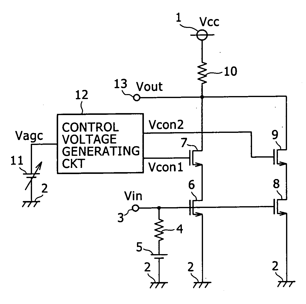
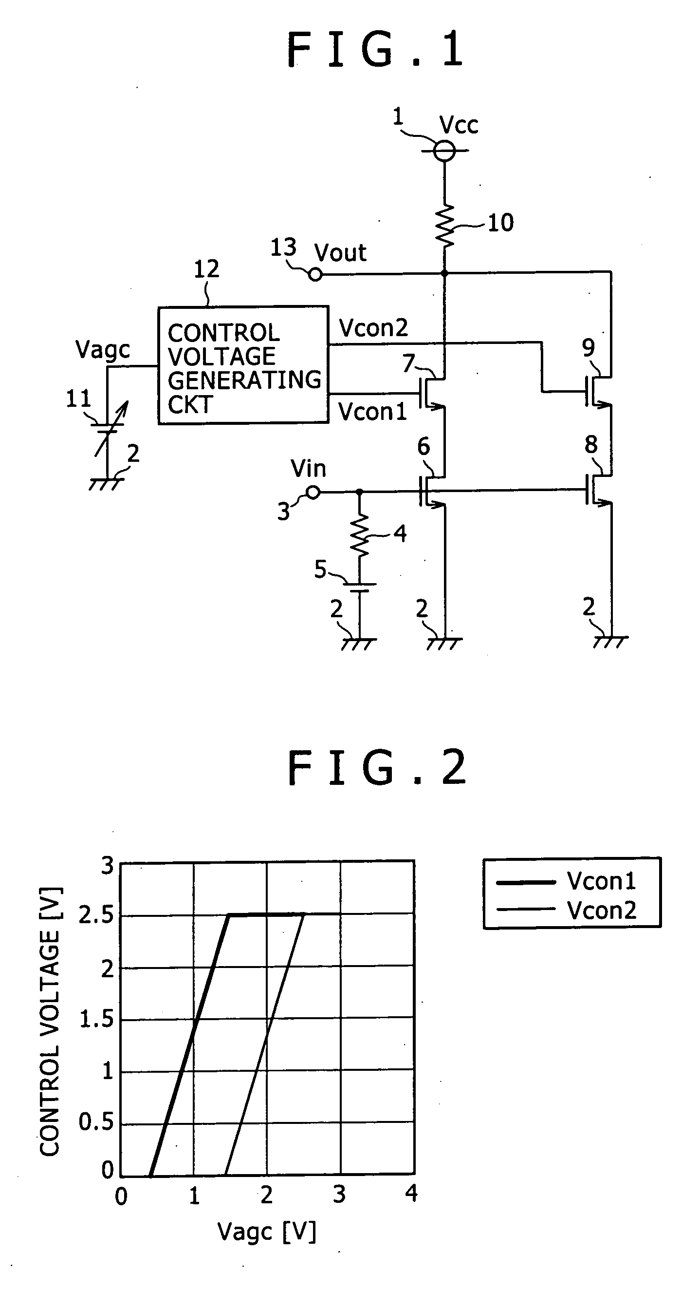
[0030]FIG. 1 is a circuit diagram showing an arrangement of a variable-gain amplifier according to a first embodiment of the present invention. In FIG. 1, the variable-gain amplifier has a voltage source 1, a ground level 2, a signal input terminal (signal input section) 3, a resistor 4 connected to the signal input terminal 3 for applying a suitable bias voltage to an input signal, a voltage source 5 for applying a suitable bias voltage, an FET (first FET) 6 having a gate connected to the signal input terminal 3 and a source connected to the ground level 2, an FET (second FET) 7 having a source connected to the drain of the FET 6, an FET (first FET) 8 having a gate connected to the signal input terminal 3 and a source connected to the ground level 2, an FET (second FET) 9 having a source connected to the drain of the FET 8, a load resistor 10 having an end connected in common to the drain of the FET 7 and the drain of the FET 9 and the other end to the voltage source 1, for extract...
second embodiment
[0040]FIG. 6 is a circuit diagram showing an arrangement of a variable-gain amplifier according to a second embodiment of the present invention. Those reference characters in FIG. 6, which are identical to those in FIG. 1, denote identical or corresponding parts,.and will not be described below. The variable-gain amplifier has a variable voltage source (voltage control means) 31 connected to the gate of the FET 7 for controlling a voltage Vcon1 to be applied to the gate thereof, a variable voltage source (voltage control means) 32 connected to the gate of the FET 9 for controlling a voltage Vcon2 to be applied to the gate thereof, a resistor 33 interposed between the signal output terminal 13 and the signal input terminal 3, and a resistor 34 interposed between the signal input terminal 3 and the ground level 2. A voltage feedback path is thus connected between the signal output terminal 13 and the signal input terminal 3 through the resistor 33 for applying a voltage-feedback gate ...
third embodiment
[0041]FIG. 7 is a circuit diagram showing an arrangement of a variable-gain amplifier according to a third embodiment of the present invention. In FIG. 7, the variable-gain amplifier has a voltage source 41, a ground level 42, a first signal input terminal 43, a second signal input terminal 44 for inputting an inverted signal which is an inversion of a signal input to the first signal input terminal 43, a resistor 45 connected to the first signal input terminal 43 for applying an appropriate bias voltage to the input signal, a resistor 46 connected to the second signal input terminal 44 for applying an appropriate bias voltage to the inverted input signal, a voltage source 47 connected to the resistor 45 and the resistor 46 for applying an appropriate bias voltage, an FET (first FET) 48 having a gate connected to the first signal input terminal 43 and a source connected to the ground level 42, an FET (second FET) 49 having a source connected to the drain of the FET 48, an FET (first...
PUM
 Abstract
Description
Claims
Application Information
 - R&D Engineer
- R&D Manager
- IP Professional
- Industry Leading Data Capabilities
- Powerful AI technology
- Patent DNA Extraction
Browse by: Latest US Patents, China's latest patents, Technical Efficacy Thesaurus, Application Domain, Technology Topic, Popular Technical Reports.
© 2024 PatSnap. All rights reserved.Legal|Privacy policy|Modern Slavery Act Transparency Statement|Sitemap|About US| Contact US: help@patsnap.com