Apparatus of ion sensitive thin film transistor and method of manufacturing of the same

a technology of ion-sensitive thin films and transistors, which is applied in the direction of sustainable manufacturing/processing, instruments, and final product manufacturing, can solve the problems of high cost and time-consuming during production, and the cost of silicon substrates is very high, and achieves the effect of low weight and low cos

Inactive Publication Date: 2006-02-16
IND TECH RES INST
View PDF11 Cites 85 Cited by
  • Summary
  • Abstract
  • Description
  • Claims
  • Application Information

AI Technical Summary

Benefits of technology

[0015] A further object of the invention is to provide an apparatus of ion sensitive thin film transistor and method of manufacturing of the same, wherein miniature, thinness, and low weight can be utilized.
[0016] ...

Problems solved by technology

Consequently, it will induce a lot of cost and time consuming during production.
Although t...

Method used


Image

  • Apparatus of ion sensitive thin film transistor and method of manufacturing of the same
  • Apparatus of ion sensitive thin film transistor and method of manufacturing of the same
  • Apparatus of ion sensitive thin film transistor and method of manufacturing of the same

Examples


Embodiment Construction

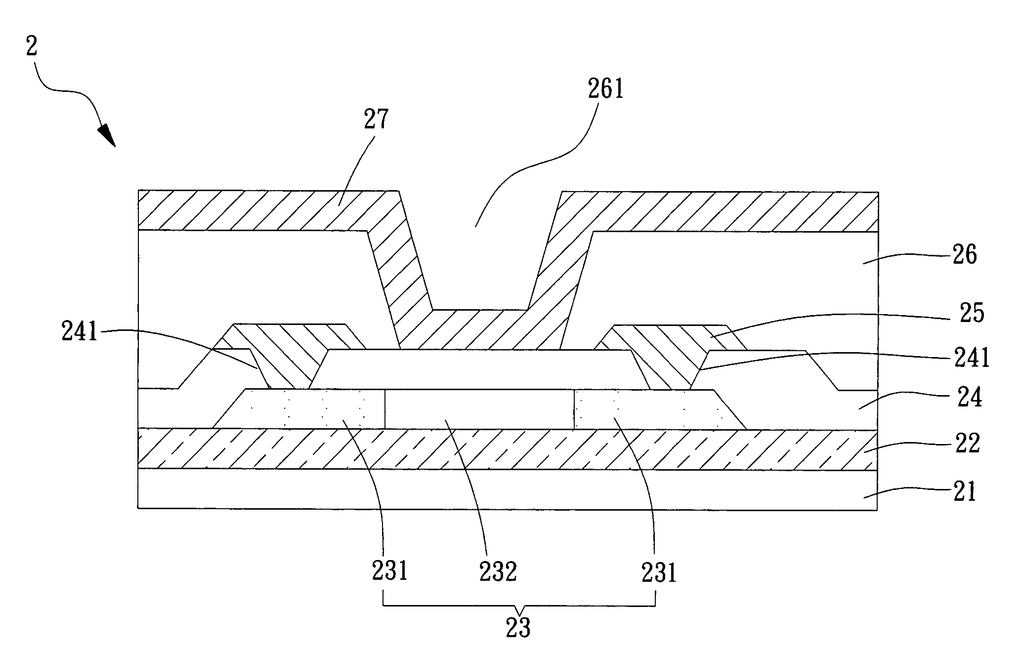
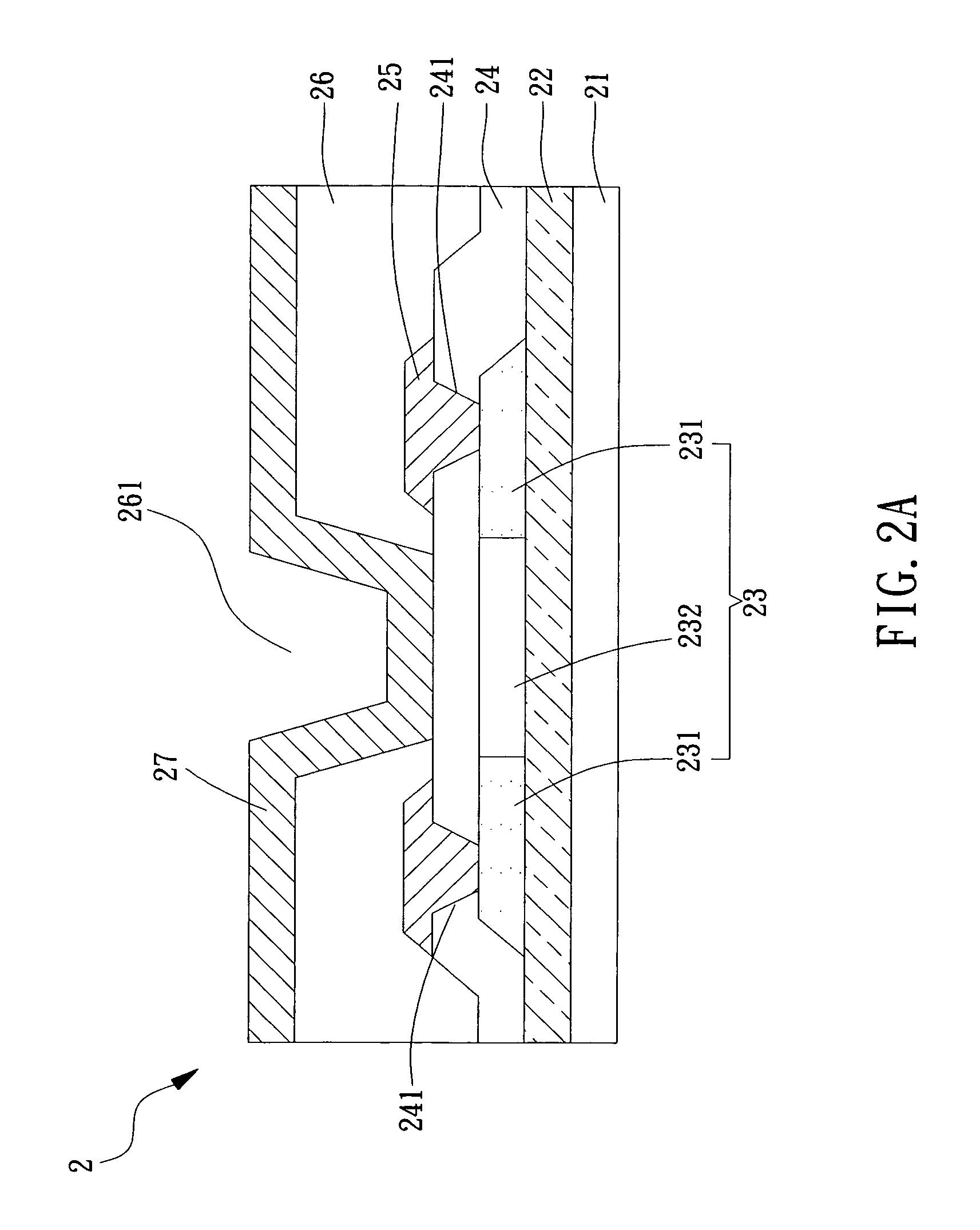
[0027] Referring to FIG. 2a, a cross-sectional view of an embodiment according to principles the invention is provided. In the figure illustrated, an apparatus of ion sensitive transistors 2 comprises: a glass substrate 21, a layer of buffer oxide 22, an active layer 23, a layer of gate oxide 24, a metal layer 25, a passivation layer 26 and a sensitive membrane 27. Said layer of buffer oxide 22 was formed on the surface of said glass substrate 21, wherein said layer of buffer oxide 22 formed on the surface of said glass substrate 21; said active layer 23, formed on the surface of said layer of buffer oxide 22, further including a pair of source / drains 231 separated from a channel region 232; said layer of gate oxide 24, formed on the surface of said active layer 23, further including contact holes 241 on said layer of gate oxide 24 set opposite to said pair of source / drains 231; said metal layer 25 formed on the surface of said layer of gate oxide 24 filling said contact hole 241 to...


PUM


Abstract

The present invention discloses an apparatus of ion sensitive thin film transistor and method of manufacturing of the same. The apparatus of the invention, formed on a glass substrate, comprises an ion detector, formed on said glass substrate, including a plurality of ion sensitive transistors and a signal processor with display, also formed on said glass substrate, being coupled with said ion detector. The signal processor with display further comprises a circuit of signal processing, a driver circuit, and a display, wherein by means of the method of Low Temperature PolySilicon, i.e. LTPS technology, the invention integrates said ion detector and said signal processor with display on said glass substrate to become an tiny, light and thin apparatus with portable and disposable characteristics.

Description

1. FIELD OF THE INVENTION [0001] The present invention relates to an apparatus of ion sensitive thin film transistor and method of manufacturing of the same. More particularly, the invention relates to utilize Low Temperature PolySilicon, i.e. LTPS, processing to integrate ion sensitive transistors, electric control circuits and display panel on a glass substrate. 2. BACKGROUND OF THE INVENTION [0002] The ISFET was first disclosed by P. Bergveld in 1970. The device is a product of applied electrochemistry and microelectronics, and has the function of ion selection and the properties of the FET. Referring to FIG. 1, the illustration describes the conventional ion sensitive transistor of the prior art. This ion sensitive transistor device is strictly different from the traditional ion selection electrode. P. Bergveld disclosed a FET, wherein the metal film set in the gate of traditional FET was removed. Furthermore, the device was immersed in electrolyte, wherein no reference electrod...

Claims


Application Information

Patent Timeline
IPC IPC(8): H01L21/00H01L23/58
CPCG01N27/414H01L27/14692H01L29/42384Y02E10/50H01L31/115H01L31/202H01L29/4908Y02P70/50
Inventor WU, YUNG FUTSAI, TZU HSUAN
Owner IND TECH RES INST
Why Eureka
Try Eureka