Light-emitting diode

a light-emitting diode and light-emitting layer technology, applied in the direction of semiconductor devices, electrical apparatus, transistors, etc., can solve the problems of wasting 80% of light generated, affecting the efficiency of light extraction, and requiring several years to put it into practical use, so as to improve the light extraction efficiency, enhance the light emission output of the light-emitting element, and alleviate the shielding of light

Inactive Publication Date: 2006-03-02
SANYO ELECTRIC CO LTD +1
View PDF5 Cites 32 Cited by
  • Summary
  • Abstract
  • Description
  • Claims
  • Application Information

AI Technical Summary

Benefits of technology

[0022] According to the present invention, the angle between a normal to the side surface, on which the light-emitting layer is exposed and which is formed as an inclined surface, of the light-emitting layer and the crystal surface on which the light-emitting layer grows is made equal to the angle at which the light emitted from the light-emitting layer is totally reflected toward the translucent substrate. Thus, the light that travels from the light-emitting layer toward the side surface of the light-emitting element has its course changed so as to be emitted through the light emission observation surface. Thus, the light emitted from the light-emitting layer is not shielded by the adhesive material, but all the light is emitted through the light emission observation surface. This enhances the light emission output of the light-emitting element.
[0023] Moreover, according to the present invention, there are provided a vertical hole so deep as to reach the first-conductivity-type semiconductor layer but not to reach the second-conductivity-type semiconductor layer and a conductive material formed along the vertical hole so as to conduct to the first-conductivity-type semiconductor layer. Thus, an electrode that conducts to the conductive material and via which a voltage is applied to the semiconductor layer can be formed on the light emission observation surface of the translucent substrate. This permits electrodes to be arranged separately on the first-surface and second-surface sides of the translucent substrate. Thus, it is possible to alleviate the shielding of light by the electrodes and thereby enhance light extraction efficiency. Moreover, wire-bonding for electrode-to-lead connection needs to be performed only at one spot. This greatly enhances assembly workability.
[0024] Moreover, according to the present invention, a vertical hole is formed to penetrate the thin first-conductivity-type semiconductor layer. This makes the light-emitting diode easy to fabricate.
[0025] Moreover, according to the present invention, a pad electrode having an area larger than the cross-sectional area of the vertical hole is provided. This permits easy wire-bonding of a lead.
[0026] Moreover, according to the present invention, the vertical hole is made increasingly small with increasing depth. This makes it easy to form a conductive material with a predetermined thickness on the inner surface of the vertical hole by vapor deposition or sputtering.
[0027] Moreover, according to the present invention, the conductive material is translucent. This reduces the absorption of light inside the vertical hole, and thus permits the light emitted by the light-emitting layer to be extracted to the outside effectively without loss.

Problems solved by technology

One of the challenges associated with various light-emitting devices such as blue light-emitting diodes and blue laser diodes is how to increase the efficiency with which light is extracted from a light-emitting element.
On the other hand, in light-emitting diodes currently being developed, about 80% of the light generated is wasted.
This makes it more difficult for electric energy to be converted into heat energy in the light-emitting layer in the light-emitting element, and thus helps increase light energy.
Such processing of a sapphire substrate, however, is still under research, and it is expected it will take several years to put that into practical use.
Moreover, in Patent Publication 1, it is stated that, from the production engineering point of view, it is impossible to apply this light-emitting diode to a light-emitting diode having a cup-shaped leadframe.

Method used


Image

  • Light-emitting diode
  • Light-emitting diode
  • Light-emitting diode

Examples


Embodiment Construction

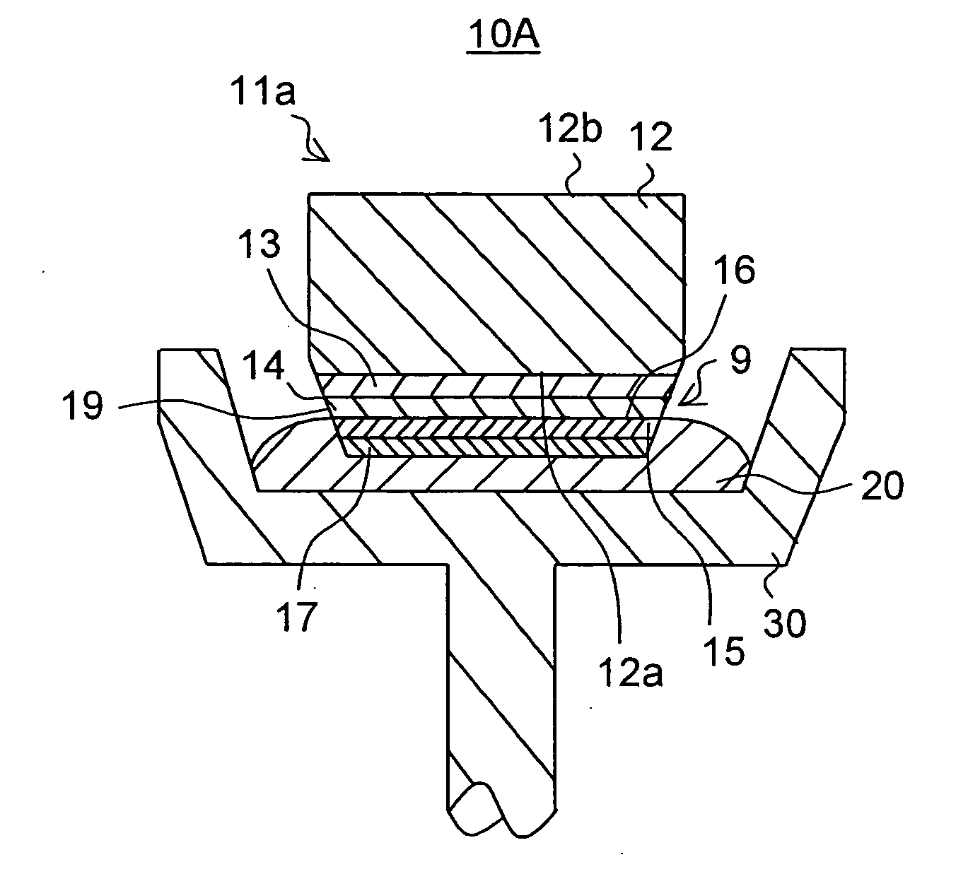
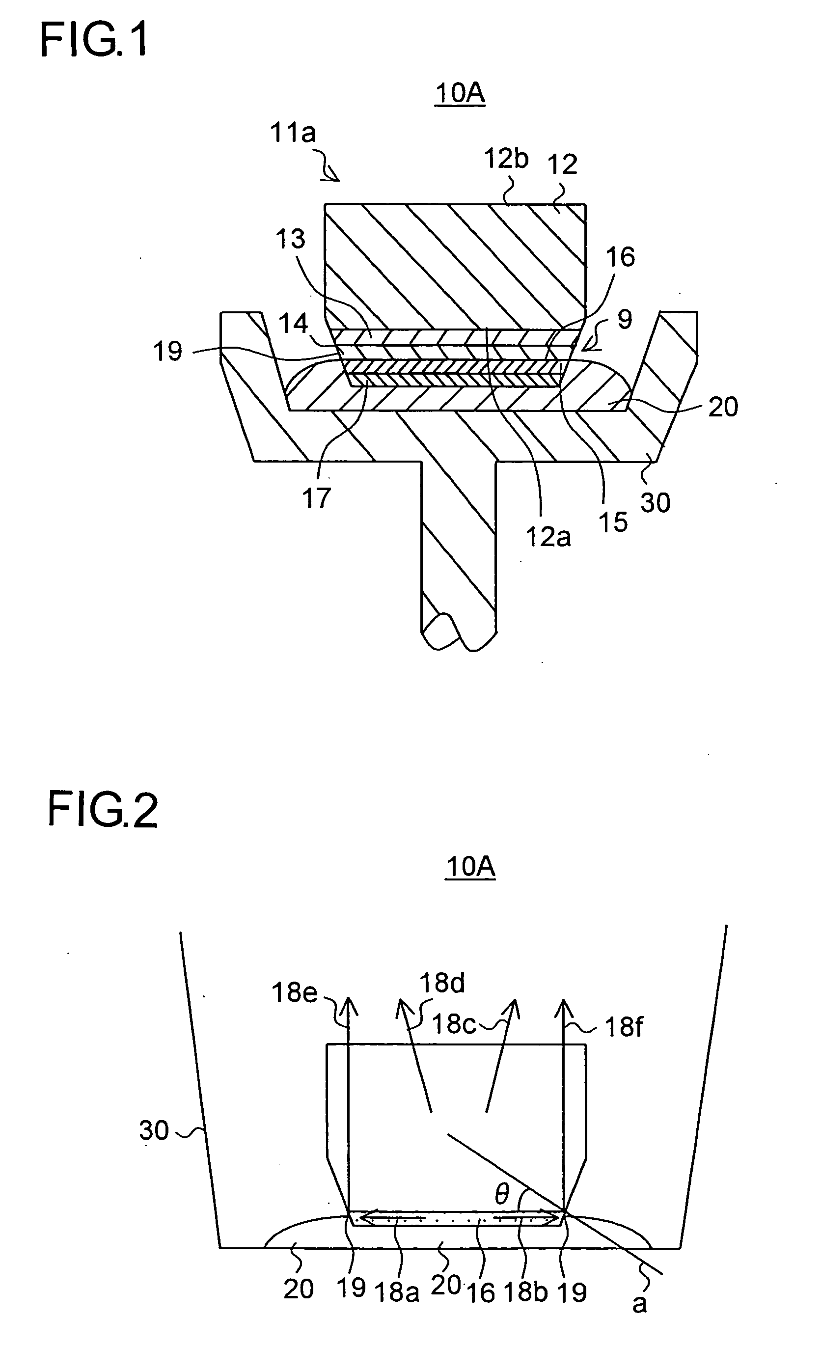
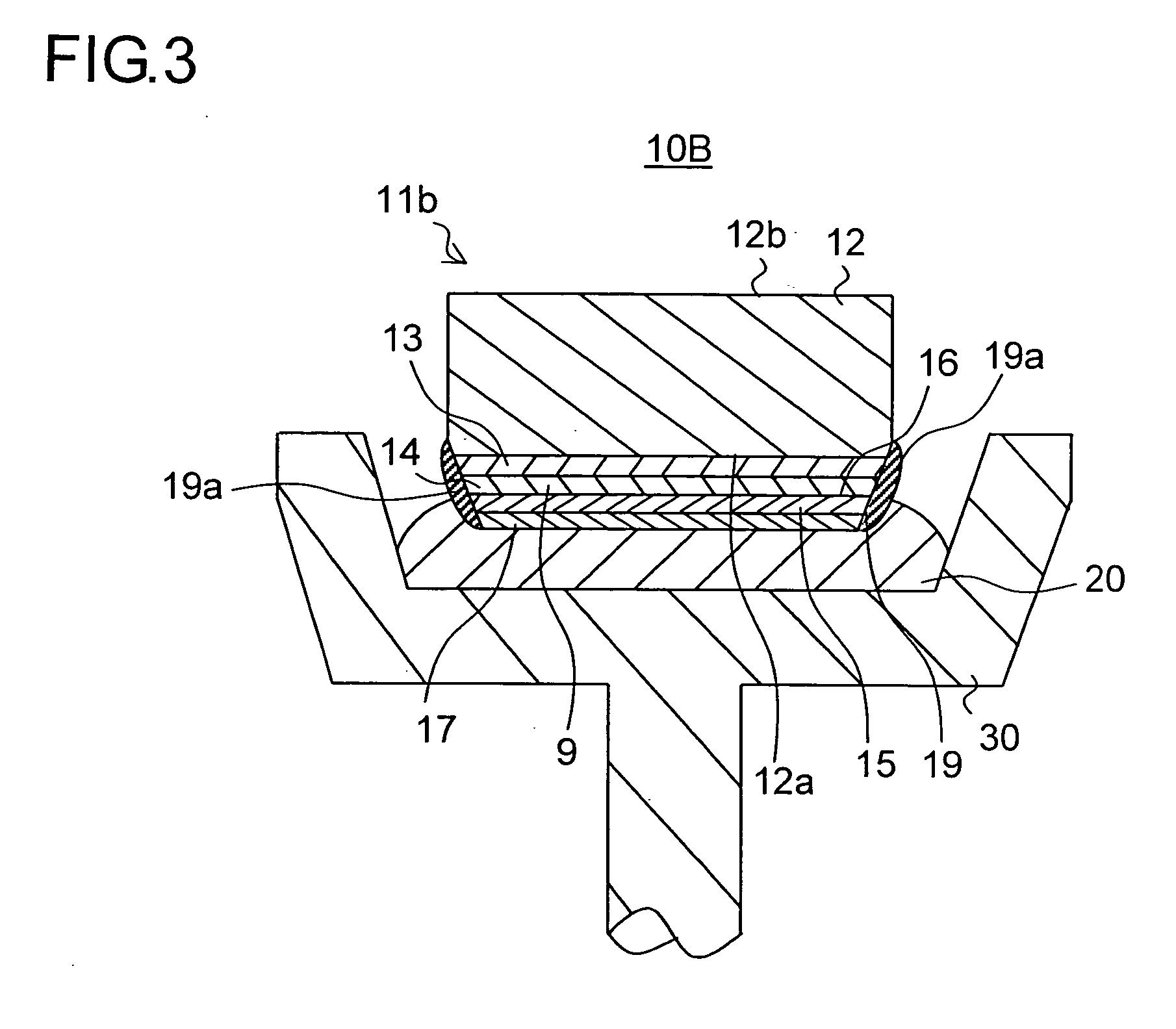
[0057] Hereinafter, embodiments of the present invention will be described with reference to the drawings. For the sake of convenience, such parts as find their counterparts in FIGS. 6 and 7 described earlier are identified with common reference symbols. It should be understood that the present invention may be implemented in any manner other than specifically shown in the drawings. FIG. 1 is a sectional view showing the light-emitting diode of a first embodiment of the invention.

[0058] The light-emitting diode 10A has an LED chip 11a provided on top of a cup-shaped leadframe 30. The LED chip 11a has a translucent substrate 12 formed of insulating sapphire, and on a first surface 12a of the sapphire substrate 12 is formed, via a butter layer 13, a semiconductor layer 9. The semiconductor layer 9 is composed of a first-conductivity-type semiconductor layer 14 formed of one of p- and n-type semiconductors and a second-conductivity-type semiconductor layer 15 formed of the other of th...


PUM


Abstract

A light-emitting diode 10A has a light-emitting element 11a fixed to a leadframe 30 with a conductive adhesive material 20, the light-emitting element 11a having a semiconductor layer 9 including a light-emitting layer 16 laid on a first surface 12a of a translucent substrate 12, a second surface 12b thereof facing away from the first surface 12a being used as a light emission observation surface. A side surface of the semiconductor layer 9 is an inclined surface inclined relative to the first surface 12a, and an angle θ between a normal “a” to the inclined surface and a crystal surface on which the light-emitting layer 16 grows is equal to an angle at which light emitted by the light-emitting layer 16 is totally reflected toward the translucent substrate 12.

Description

TECHNICAL FILED [0001] The present invention relates to a light-emitting diode having a light-emitting element composed of a semiconductor layer laid on top of a translucent substrate. BACKGROUND ART [0002] One of the challenges associated with various light-emitting devices such as blue light-emitting diodes and blue laser diodes is how to increase the efficiency with which light is extracted from a light-emitting element. The light emission efficiency of, in particular, white light-emitting diodes has been improving year after year, almost doubling every two years. Even with this fast improvement, it is said it will take another several years to overtake the light emission efficiency, 60 lm / W, of fluorescent lamps commonly used in households. [0003] On the other hand, in light-emitting diodes currently being developed, about 80% of the light generated is wasted. The part of the light that does not go out of the light-emitting element undergoes repeated multiple reflection inside t...

Claims


Application Information

Patent Timeline
Patent Type & Authority Applications(United States)
IPC IPC(8): H01L31/112H01L33/20H01L33/38
CPCH01L33/20H01L33/382H01L24/32H01L2224/48091H01L2224/73265H01L2224/48247H01L2924/00014H01L2924/12041H01L2924/15787
Inventor MATSUSHITA, YASUHIKO
Owner SANYO ELECTRIC CO LTD
Why Eureka
Try Eureka