
Semiconductor device and fabrication method of the same

a technology of semiconductor devices and fabrication methods, applied in the direction of semiconductor devices, basic electric elements, electrical equipment, etc., can solve the problems of steep curvature of portions, difficulty in allowing the depletion layer to sufficiently spread, and the ring structure taught thereby

Inactive Publication Date: 2006-03-02
KK TOSHIBA
View PDF3 Cites 141 Cited by
  • Summary
  • Abstract
  • Description
  • Claims
  • Application Information

AI Technical Summary

Benefits of technology

[0010] According to still another aspect of the present invention, there is provided a method for fabricating a semiconductor device comprises, forming a to-be-processed film to be processed into a mask on a surface of a semiconductor layer including a terminate end part and a cell formation part as surrounded by this end part, forming at a portion of the to-be-processed film corresponding to the end part a plurality of openings surrounding a portion of the to-be-processed film corresponding to the ce

Problems solved by technology

This would result in occurrence of portions with steep curvatures.
Unfortunately, the prior known guard ring structures as taught thereby are faced with the difficulty to permit the depletion layer to sufficiently spread at the end part.

Method used


Image

  • Semiconductor device and fabrication method of the same
  • Semiconductor device and fabrication method of the same
  • Semiconductor device and fabrication method of the same

Examples


first embodiment

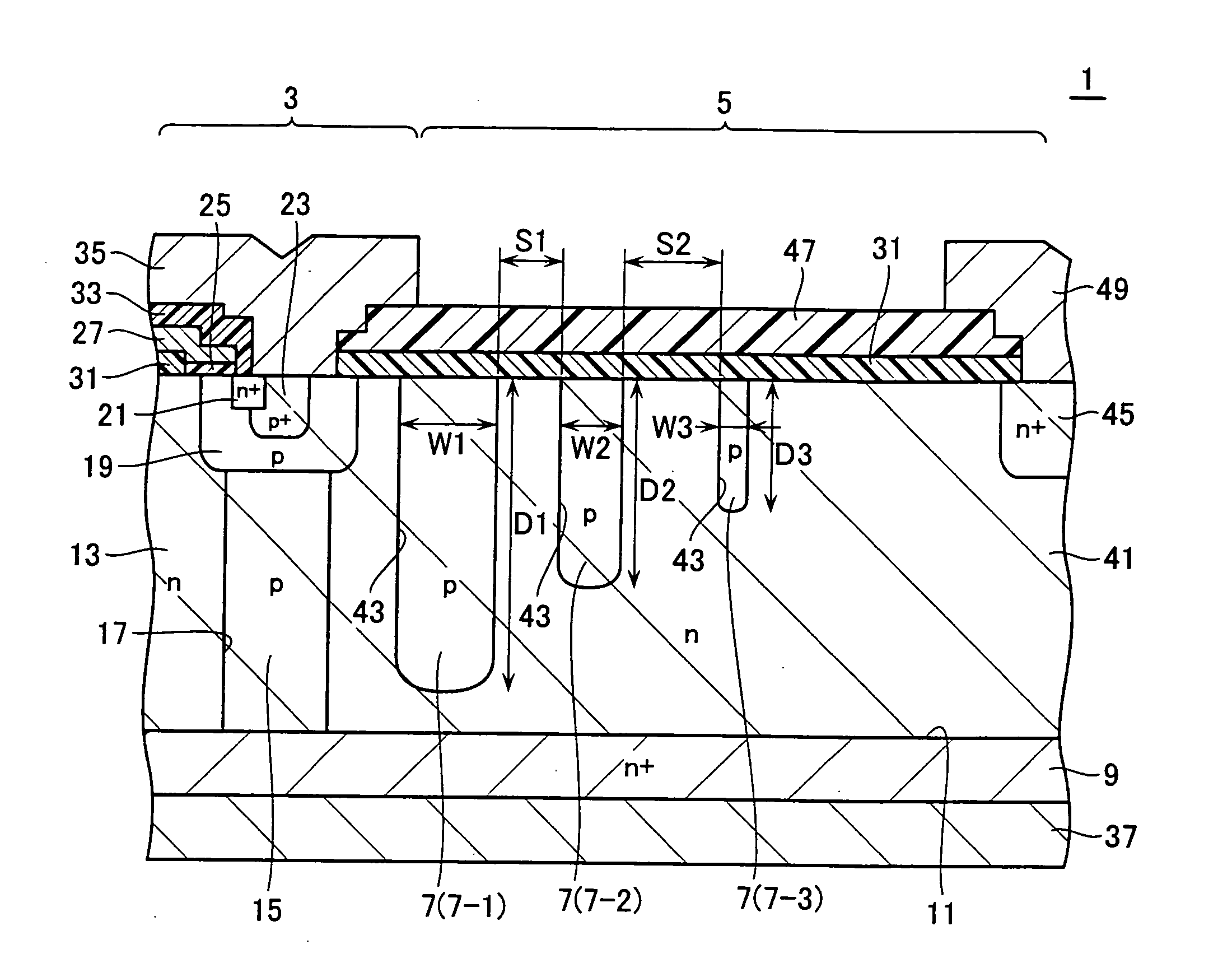
[0033] A main feature of a semiconductor device in accordance with a first embodiment lies in that a plurality of guard rings are formed at a terminate end part so that these are made (1) shallower, (2) smaller in width and (3) larger in interval of neighboring guard rings as they get near to a guard ring that is located on an outer side.

[0034] (Semiconductor Device Structure)

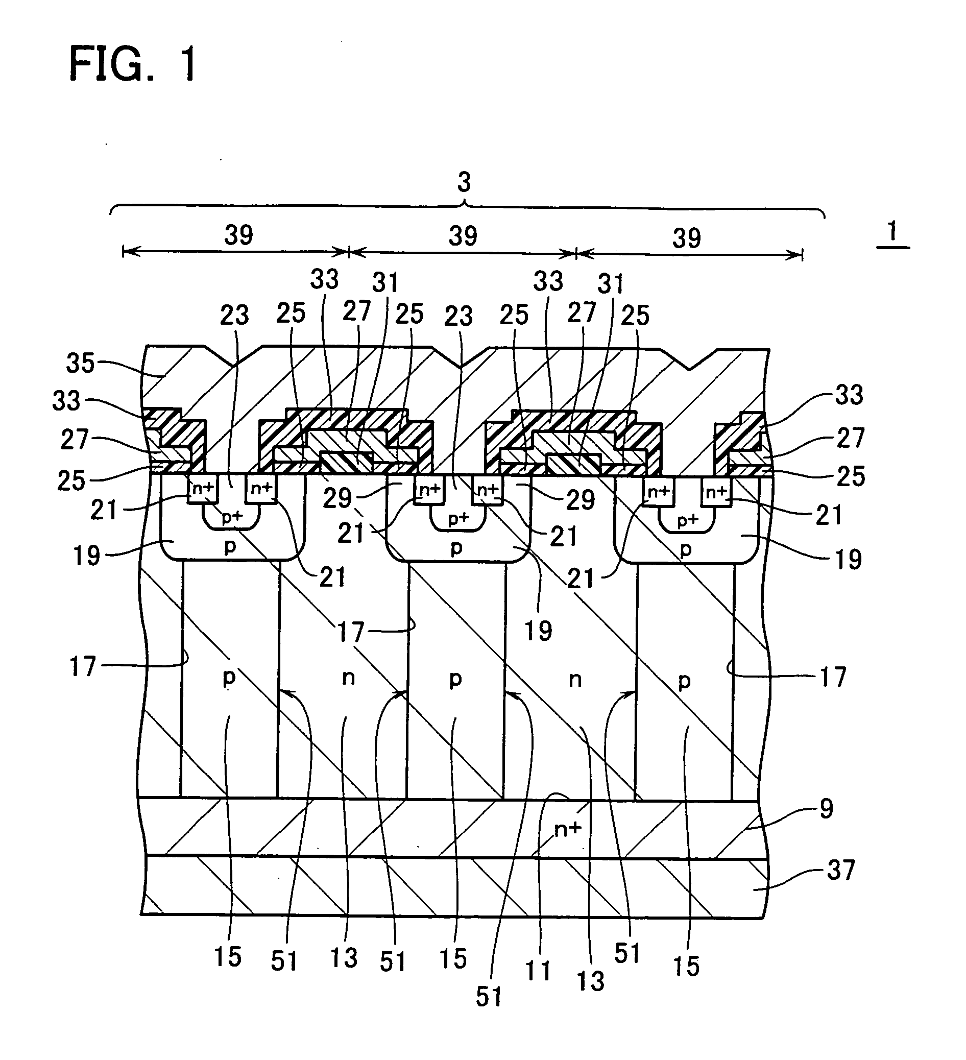
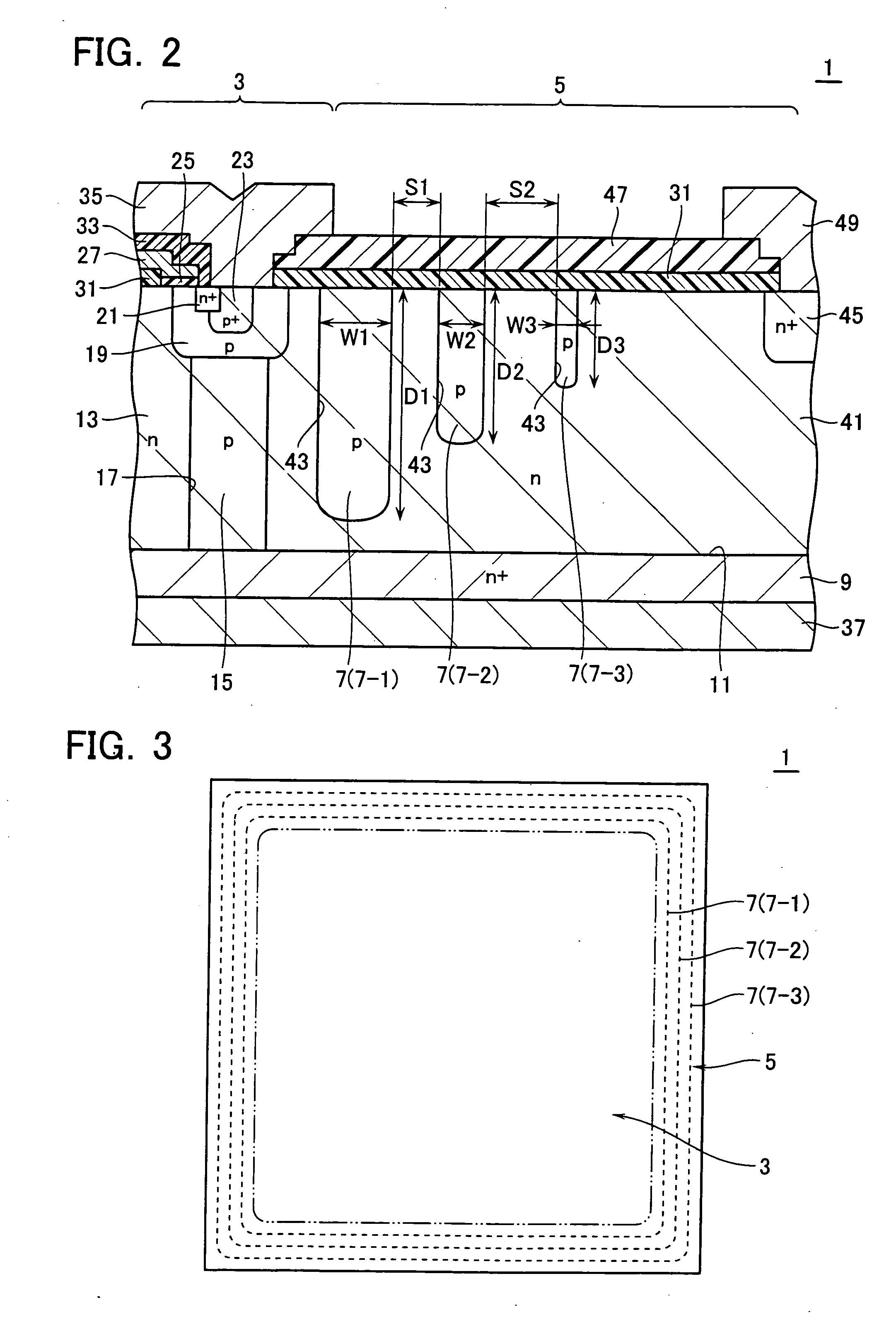
[0035]FIG. 1 is a diagram showing a partial cross-sectional view of a cell formation part 3 of a semiconductor device 1 for the power use in accordance with the first embodiment, and FIG. 2 shows a partial cross-section of a terminate end part 5 of the power semiconductor device 1. FIG. 3 depicts a plan view of the semiconductor device 1. Firstly, a planar structure of semiconductor device 1 will be explained using FIG. 3. The power semiconductor device 1 is a semiconductor chip which includes a terminate end part 5 and a cell formation part 3 as surrounded by this end part 5 In the cell formation part 3, a g...

second embodiment

[0076]FIG. 19 is a partial cross-sectional view of the end part 5 of a power semiconductor device 71 in accordance with a second embodiment of the invention. In the first embodiment shown in FIG. 2, the multiple trenches 17 and 43 are formed in the single-crystalline silicon layer 41 while letting these trenches be filled with buried epitaxial growth layers, which are opposite in conductivity type to the silicon layer 41. This results in formation of the super-junction structure in the cell formation part 3 while at the same time forming guard rings 7 in the end part 5.

[0077] By contrast, the second embodiment shown in FIG. 19 is with repeated execution of a necessary number (five times in the second embodiment) of process steps of forming an n-type single-crystalline silicon layer by epitaxial growth techniques, selectively implanting a p-type impurity into this layer, and then activating this impurity. By repeating this process, the super-junction structure is formed in the cell ...


PUM


Abstract

A semiconductor device comprises a semiconductor layer which includes a terminate end part and a cell formation part that is surrounded by this end part, and a plurality of guard rings each of which is formed at the end part to surround the cell formation part. These guard rings are made shallower and smaller in width as they get near to the guard ring that resides at the outside position.

Description

CROSS-REFERENCE TO RELATED APPLICATION(S) [0001] This application is based upon and claims the benefit of priority from the prior Japanese Patent Application No. 2004-254467, filed on Sep. 1, 2004, the entire contents of which are incorporated herein by reference. BACKGROUND OF THE INVENTION [0002] 1. Field of the Invention [0003] The present invention relates to semiconductor devices such as metal oxide semiconductor field effect transistors (MOSFETs) for the power use. This invention also relates to fabrication methodology of the same. [0004] 2. Description of the Related Art [0005] Semiconductor devices for the power use, such as power MOSFETs, are semiconductor chips that are structured so that a large number of cells are formed in an epitaxially grown layer (semiconductor region) that is disposed on or above a semiconductor substrate while letting the gates of such cells be common-coupled together. As power MOSFETs are low in turn-on (ON) resistance and are capable of performin...

Claims


Application Information

Patent Timeline
IPC IPC(8): H01L29/76H01L21/336
CPCH01L29/0634H01L29/42368H01L29/0619H01L29/7811H01L29/66712
Inventor TSUCHITANI, MASANOBUMATSUDA, TETSUOOKUMURA, HIDEKIYAMASHITA, ATSUKO
Owner KK TOSHIBA
Learn More