Sensor package

a technology of sensor package and package, which is applied in the direction of semiconductor/solid-state device details, electrical apparatus, semiconductor devices, etc., can solve the problems of limiting the height (distance between the lens and the substrate) and affecting the quality of the image sensor package b>10/b>

Inactive Publication Date: 2006-03-02
HIMAX TECH LTD
View PDF20 Cites 51 Cited by
  • Summary
  • Abstract
  • Description
  • Claims
  • Application Information

AI Technical Summary

Benefits of technology

[0010] It is an object of the present invention to provide an image sensor package including a spacer capable of controlling a gap between a transparent substrate unit and an image sensor and further maintaining the gap between the transparent substrate unit and the image sensor.

Problems solved by technology

However, the image sensor package 10 is restricted in its design because the chip 30 is disposed on the substrate 20 by using the wire bonding process, and thus the entire height (distance between the lens and the substrate) of the image sensor package 10 is too long, such that the volume of the image sensor package 10 will be enlarged.
Furthermore, the image sensor package 10 cannot be applied to the mass production with wafer lever, such that the cost of the packaging process is increased and the reliability of package is decreased.
However, the bumps and the adhesive layer are only used for electrically connecting the pads to the printed circuit board, but they are not used for controlling the gap between the diced wafer and the diced transparent substrate.
Thus, the non-uniform thickness of the adhesive layer located between the diced wafer and the diced transparent substrate affects the optical effect of the image sensor and the emitting light.
However, when the first glass substrate is attached to the wafer, the first adhesive will be pressed and is non-uniform in its thickness.
The non-uniform thickness of the first adhesive layer affects the optical effect of the image sensor and the emitting light.

Method used


Image

  • Sensor package
  • Sensor package
  • Sensor package

Examples


first embodiment

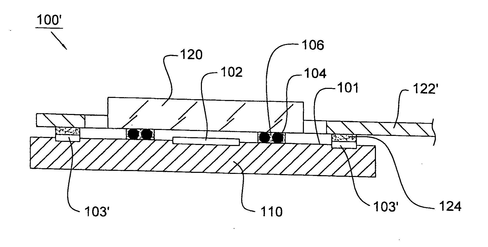
[0030] Referring to FIGS. 4a and 4b, they depict an image sensor package 100 according to the present invention. The image sensor package 100 includes a chip 110, which includes an active surface 101, an image sensor 102 disposed on the active surface 101, and a plurality of pads 103 disposed on the active surface 101, wherein the pads 103 and the image sensor 102 are at the same side. A transparent substrate unit 120 is disposed above the active surface 101 of the chip 110 and covers the image sensor 102. The image sensor 102 can be a complementary metal-oxide semiconductor (CMOS) or charge coupled device (CCD), which made of semiconductor material or organic semiconductor material such as pentacene (C22H14). The chip 110 can be made from a transparent substrate, such as glass, acrylic resin, sapphire, ployimide or silicon wafer. The transparent substrate unit 120 can be made of glass, acrylic resin, sapphire or ployimide materials. A plurality of spacers 104 are disposed between t...

second embodiment

[0042] Referring to FIGS. 13a and 13b, they depict an image sensor package 200 according to the present invention. The image sensor package 200 is similar to the image sensor package 100 wherein the similar elements are designated with the similar reference numerals. The image sensor package 200 includes a chip 210, which includes an active surface 201, an image sensor 202 disposed on the active surface 201, and a plurality of pads 203 disposed on the active surface 201, wherein the pads 203 and the image sensor 202 are at the same side. A transparent substrate unit 220 is disposed above the active surface 201 of the chip 210 and covers the image sensor 202. An annular spacer 204 is regarded as a plurality of spacers which are connected to one another and encloses the image sensor 202, and the annular spacer 204 is disposed between the transparent substrate unit 220 and the chip 210 for maintaining a predetermined gap defined between the transparent substrate unit 220 and the image ...

third embodiment

[0054] Referring to FIG. 21, it depicts an image sensor package 300 according to the present invention. The image sensor package 300 includes a chip 370, which includes an active surface 301, an image sensor 362 disposed on the active surface 301, and a plurality of pads 363 disposed on the active surface 301. A pad extended layer 364 is disposed on the active surface 301 of the chip 370 and is electrically connected to the pads 363. A first glass substrate unit 368 is located on the active surface 301 of the chip 370 and covers the image sensor 362. The image sensor 362 can be a complementary metal-oxide semiconductor (CMOS) or charge coupled device (CCD), which made of semiconductor material or organic semiconductor material such as pentacene (C22H14). The first transparent substrate unit 368 can be made of glass, acrylic resin, sapphire or ployimide materials. The chip 370 can be made from a transparent substrate, such as glass, acrylic resin, sapphire, ployimide or silicon wafer...


PUM


Abstract

An image sensor package includes a bottom substrate, a transparent substrate, a plurality of spacers and adhesive. The bottom substrate includes a plurality of chips, which each includes an active surface and an image sensor disposed on the active surface. The transparent substrate includes a plurality of transparent substrate units which are respectively corresponding to the chips, wherein each transparent substrate unit is disposed above the active surface of the chip and covers the image sensor. The spacers are disposed between the transparent substrate unit and the chip for maintaining a predetermined gap between the transparent substrate unit and the image sensor. Each transparent substrate unit and chip are connected to each other by the adhesive.

Description

[0001] This application claims the priority benefit of Taiwan Patent Application Serial Number 093125403, filed Aug. 24, 2004, the full disclosure of which is incorporated herein by reference. BACKGROUND OF THE INVENTION [0002] 1. Field of the Invention [0003] The present invention generally relates to a sensor package, and more particularly to an image sensor package including a spacer for maintaining a predetermined gap defined between a transparent substrate unit and an image sensor. [0004] 2. Description of the Related Art [0005] For image sensors such as complementary metal-oxide semiconductors (CMOS), the manufacturing technology of the image sensors is similar to that of typical semiconductor chips, and the image sensor is a semiconductor mainly made of silicon and germanium elements. The complementary metal-oxide semiconductor includes a N-type metal-oxide semiconductor (NMOS) transistor with negative electricity and a P-type metal-oxide semiconductor (PMOS) transistor with ...

Claims


Application Information

Patent Timeline
Patent Type & Authority Applications(United States)
IPC IPC(8): H01L23/02
CPCH01L27/14618H01L27/14625H01L2924/10253H01L2924/1815H01L2224/32013H01L2224/48465H01L27/14634H01L27/14636H01L27/14683H01L27/1469H01L31/0203H01L2224/32225H01L2224/48227H01L2924/00
Inventor LIU, CHUNG YUAN
Owner HIMAX TECH LTD
Why Eureka
Try Eureka