Variable threshold transistor for the Schottky FPGA and multilevel storage cell flash arrays

Inactive Publication Date: 2006-03-02
SUPER TALENT ELECTRONICS
View PDF3 Cites 40 Cited by
  • Summary
  • Abstract
  • Description
  • Claims
  • Application Information

AI Technical Summary

Benefits of technology

[0006] An IC solution utilizing mixed FPGA and MLC arrays is proposed. The process technology is based on the Schottky CMOS devices comprising of CMOS transistors, low barrier Schottky barrier diode (SBD), and multi-level cell (MLC) flash transistors. Circuit architecture are based on the pulsed Schottky CMOS Logic (SCL) gate arrays, wherein a variable threshold NMOS transistor may replace the regular switching transistor. During initialization windows, existing FPGA programming techniques can selectively adjust the VT of the switching transistor, re-configure the intra-connections of the simple SCL gates, complete all global interconnections of various units. Embedded hardware ar

Problems solved by technology

However, little work was developed to employ

Method used


Image

  • Variable threshold transistor for the Schottky FPGA and multilevel storage cell flash arrays
  • Variable threshold transistor for the Schottky FPGA and multilevel storage cell flash arrays
  • Variable threshold transistor for the Schottky FPGA and multilevel storage cell flash arrays

Examples


Embodiment Construction

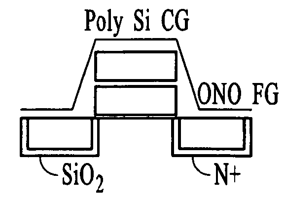
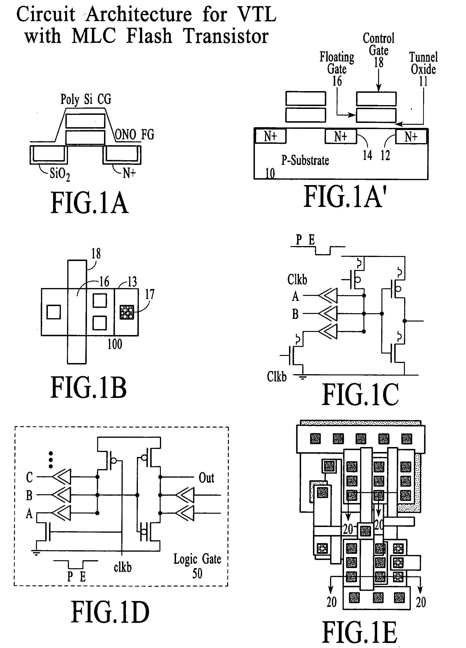
[0040] The present invention relates generally to the mixed logic and memory devices in single chip and more particularly to the use of variable threshold transistors for low power logic and multilevel storage cell (MLC) arrays. The following description is presented to enable one of ordinary skill in the art to make and use the invention and is provided in the context of a patent application and its requirements. Various modifications to the preferred embodiment and the generic principles and features described herein will be readily apparent to those skilled in the art. Thus, the present invention is not intended to be limited to the embodiment shown but is to be accorded the widest scope consistent with the principles and features described herein.

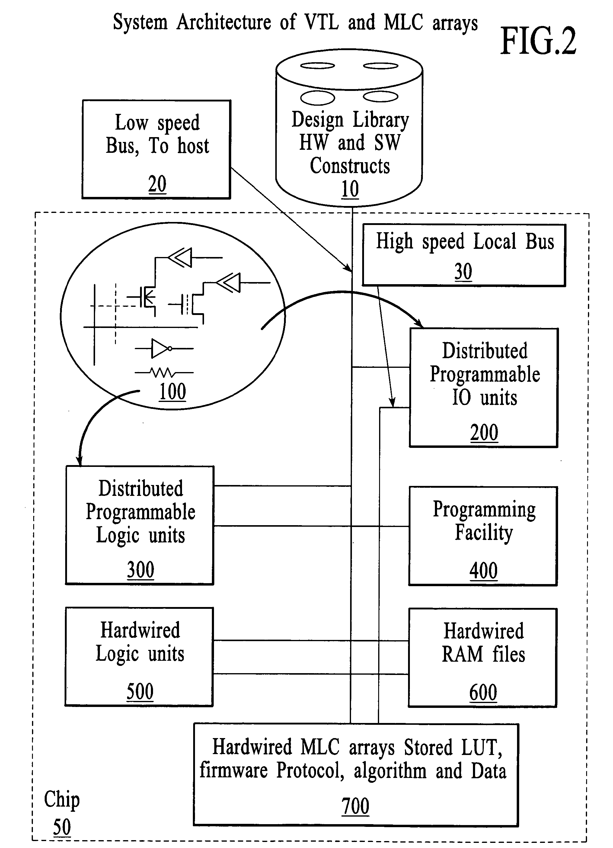
1. The Variable Threshold Transistor for VTL and MLC arrays

[0041] A device process, circuit, and system architecture of combined FPGA and EEPROM mass storage techniques in accordance with the present invention that will support both ...


PUM


Abstract

An IC solution utilizing mixed FPGA and MLC arrays is proposed. The process technology is based on the Schottky CMOS devices comprising of CMOS transistors, low barrier Schottky barrier diode (SBD), and multi-level cell (MLC) flash transistors. Circuit architectures are based on the pulsed Schottky CMOS Logic (SCL) gate arrays, wherein a variable threshold NMOS transistor may replace the regular switching transistor. During initialization windows, existing FPGA programming techniques can selectively adjust the VT of the switching transistor, re-configure the intra-connections of the simple SCL gates, complete all global interconnections of various units. Embedded hardware arrays, hardwired blocks, soft macro constructs in one chip, and protocols implementations are parsed. A wide range of circuit applications involving generic IO and logic function generation, ESD and latch up protections, and hot well biasing schemes are presented. The variable threshold transistors thus serve 3 distinctive functions. It acts as an analog device to store directly nonvolatile information in SCL gates. It couples the diode tree logic functions. Finally, it stores and operates large amount of information efficiently. The mixed SCL type FPGA and MLC storages shall emerge as the most compact logic and memory arrays in Si technology. Low power, high performance, and high capacity ICs are designed to mix and replace conventional CMOS-TTL circuits. The idea of multi-value logic composed of binary, ternary, and quaternary hardware and firmware is also introduced.

Description

FIELD OF THE INVENTION [0001] The present invention relates generally to the mixed logic and memory devices in single chip and more particularly to the use of variable threshold transistors for low power logic and multilevel storage cell (MLC) arrays. BACKGROUND OF THE INVENTION 1. Mixed Signal Circuits for Super IC [0002] The electrical erasable and programmable EEPROM memory has received wide attention in the last decade. Both the technological advances and broad product applications has made it the most emerging candidate for implementing SOC level memory component integrations. [0003] On the process and device technology front, the general practice has been focused on the miniaturization of the physical size of the storage bit, scaling down the cell operating voltages and currents and therefore lowering power consumptions, implementing multilevel signal storages per physical cell area, building up on chip apparatus to manage per bit, byte, large and partial arrays, resource sha...

Claims


Application Information

Patent Timeline
IPC IPC(8): H03K19/00
CPCH01L27/0207H01L27/11807H01L27/1203H03K19/0956H03K3/037H03K19/0002H03K3/0315
Inventor CHANG, AUGUSTINE W.
Owner SUPER TALENT ELECTRONICS
Why Eureka
Try Eureka