Spin injection device, magnetic device using the same, magnetic thin film used in the same

a technology of magnetic thin film and injection device, which is applied in the direction of nanoinformatics, magnetic bodies, instruments, etc., can solve the problems of not being able to obtain half metal as an actual thin film, not being able to guarantee half metal as bulk material, etc., to achieve low external magnetic field, high speed, and large capacity

Inactive Publication Date: 2006-03-02
JAPAN SCI & TECH CORP
View PDF3 Cites 82 Cited by
  • Summary
  • Abstract
  • Description
  • Claims
  • Application Information

AI Technical Summary

Benefits of technology

[0034] A tunnel magnetoresistance effect device as set forth in claim 26 is characterized in that it has a plurality of ferromagnetic layers on a substrate, at least one of the ferromagnetic layers is Co2FexCr1-xAl magnetic thin film (where 0≦x≦1) having either one of structures L21, B2, and A2. Said ferromagnetic layer consists of a fixed and a free layers, and said free layer is preferably Co2FexCr1-xAl magnetic thin film (where 0≦x≦1) having either one of structures L21, B2, and A2. Co2FexCr1-xAl thin film can be formed without heating a substrate. In this case, the substrate may be either one of thermally oxidized Si, glass, MgO single crystal, GaAs single crystal, or Al2O3 single crystal. The buffer layer may be provided between the substrate and Co2FexCr1-xAl thin film. Said buffer layer may be made up with at least one of Al, Cu, Cr, Fe, Nb, Ni, Ta, and NiFe. According to the aspect mentioned above, the tunnel magnetoresistance effect device with large TMR in low external magnetic field can be obtained at room temperature.
[0035] A giant magnetoresistance effect device is characterized in that it has a plurality of ferromagnetic layers on a substrate, at least one of the ferromagnetic layers consists of Co2FexCr1-xAl magnetic thin film (where O≦x≦1) having either one of structures L21, B2, and A2, and has the structure in which electric current flows in the direction perpendicular to film surface. Said ferromagnetic layer consists of a fixed and a free layers, and said free layer is preferably Co2FexCr1-xAl magnetic thin film (where 0≦x≦1) having either one of structures L21, B2, and A2. Said Co2FexCr1-xAl thin film can be formed without heating a substrate. The buffer layer may be provided between the substrate and Co2FexCr1-xAl thin film. As the substrate, either one of thermally oxidized Si, glass, MgO single crystal, GaAs single crystal, or Al2O3 single crystal may be used. Said buffer layer may be made up with at least one of Al, Cu, Cr, Fe, Nb, Ni, Ta, and NiFe. According to the aspect mentioned above, the giant magnetoresistance effect device with large GMR in low external magnetic field can be obtained at room temperature.
[0036] A magnetic device as set forth in claim 38 is characterized in that it is formed with Co2FexCr1-xAl magnetic thin film (0≦x≦1) having either of structures L21, B2, and A2 being formed on a substrate. In this case, the tunnel magnetoresistance effect device or the giant magnetoresistance effect device, of which a free layer is made of said Co2

Problems solved by technology

Therefore, a half metal as bulk material is not guaranteed to be half metal as thin film.
Even more, if the theoretical calculation of band structure shows a half metal, a half metal is not guaranteed to be obtained as an actual thin film.
This is proved by the fact that the above-mentioned various hal

Method used


Image

  • Spin injection device, magnetic device using the same, magnetic thin film used in the same
  • Spin injection device, magnetic device using the same, magnetic thin film used in the same
  • Spin injection device, magnetic device using the same, magnetic thin film used in the same

Examples


example 1

[0129] Example 1 is explained next. Example 1 corresponds to the structure of the spin injection device 14 as shown in FIG. 4.

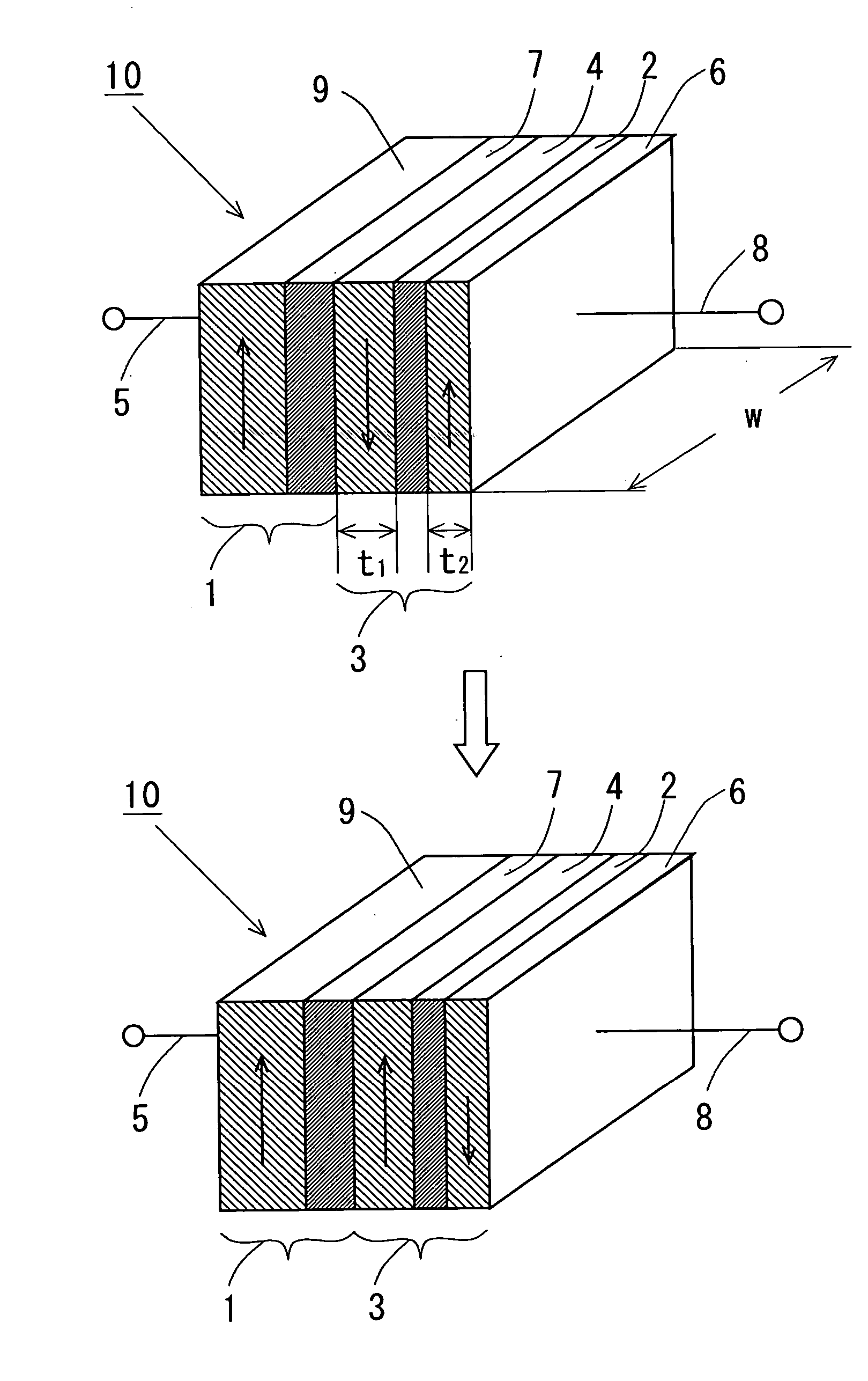
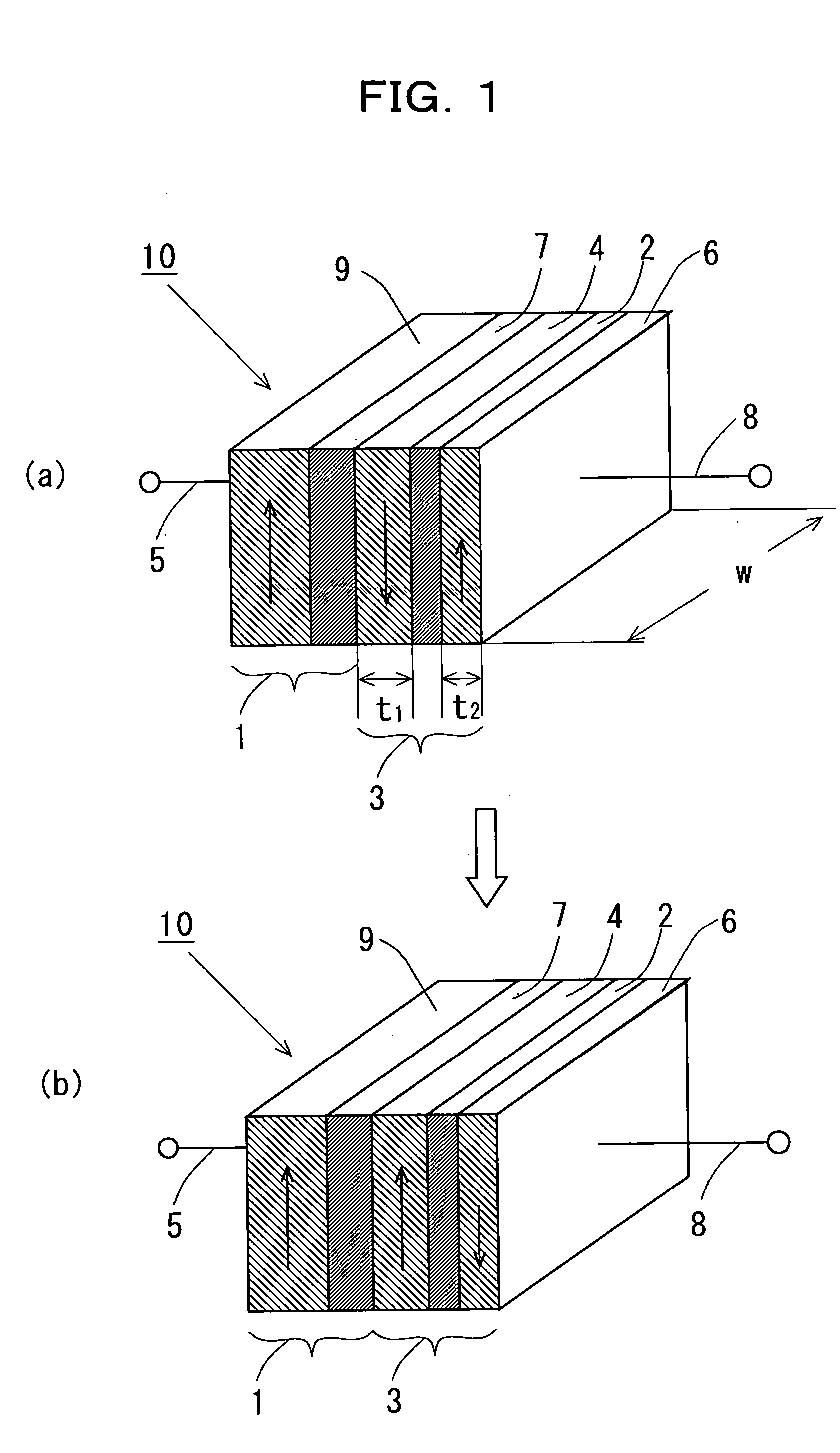
[0130] By using magnetron sputtering method, Ta (2 nm) / Cu (20 nm) / IrMn (10 nm) / Co90Fe10 (5 nm) / Cu (6 nm) / Co90Fe10 (2.5 nm) / Ru (0.45 nm) / Cu (5 nm) / Ta (2 nm) were sputtered in this order onto a thermally oxidized Si substrate. Here, the Ta and Cu layers on the thermally oxidized Si substrate and the top most layers are electrode layers. IrMn and Co90Fe10 layers are a spin polarization part 9 made of an antiferromagnetic layer 21 and a ferromagnetic fixed layer 26, respectively. Cu is an injection junction part 7. Co90Fe10 as Co alloy and Ru are a ferromagnetic free layer 27 and a nonmagnetic layer 28 provided onto Cu of a nonmagnetic layer 7.

[0131] Next, this film was microprocessed using the electron beam lithography and Ar ion milling, to fabricate a spin injection device 14 shown in FIG. 4. The device size was 300×100 nm2.

[0132]FIG. 18 shows the spin inje...

example 2

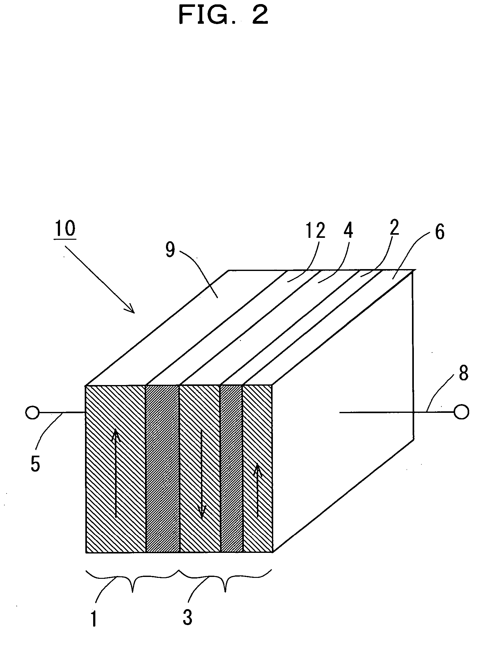
[0134] Example 2 is explained next. Example 2 corresponds to the structure of the spin injection device 16 as shown in FIG. 6. By using magnetron sputtering method, Ta (2 nm) / Cu (20 nm) / IrMn (10 nm) / Co90Fe10 (5 nm) / Cu (6 nm) / Co90Fe10 (2.5 nm) / Ru (6 nm) / Co90Fe10 (5 nm) / Cu (5 nm) / Ta (2 nm) were sputtered in this order on a thermally oxidized Si substrate. Here, the Ta and Cu layers on the thermally oxidized Si substrate and on the top most layer is the electrode layer. IrMn and Co90Fe10 layers are the spin polarization part 9 made of the antiferromagnetic layer 21 and the ferromagnetic fixed layer 26, respectively. Cu is the injection junction part 7. Co90Fe10 as Co alloy, Ru, and Co90Fe10 are the ferromagnetic free layer 27, the nonmagnetic layer 28, and a ferromagnetic layer 29 provided onto Cu of the nonmagnetic layer 7, respectively.

[0135] The difference of the spin injection device 16 of Example 2 from that 14 of example 1 is that the film thickness of Ru 28 on Co90Fe10 27 was m...

example 3

[0137] Example 3 is explained next. Example 3 corresponds to the structure shown in FIG. 8. By using magnetron sputtering method, Cu (100 nm) / NiFe (3 nm) / IrMn (10 nm) / Co90Fe10 (3 nm) was fabricated first on a thermally oxidized Si substrate, and then the 3 nm thick SiO2 was sputtered on said film, and further Co90Fe10 (1 nm) / Ru (0.45 nm) / Co90Fe10 (1.5 nm) / SiO2 (3 nm) were sputtered. Next, as the upper magnetic layer, Co90Fe10 (10 nm) / IrMn (10 nm) / Ta (5 nm) film was deposited.

[0138] As the result of transmission electron microscope observation of the cross section of said film, Co90Fe10 (1 nm) / Ru (0.45 nm) / Co90Fe10 (1.5 nm) was particulate merged layer as only one layer in SiO2, and it was seen to be a double tunnel structure with SiO2 as insulating matrix. In said structure, the electric current flew by applying voltage between Cu and Ta films. And the resistance at that time was observed at room temperature with current varied, then as the result, the jump of resistance was observ...


PUM


Abstract

A spin injection device capable of spin injection magnetization reversal at low current density, a magnetic apparatus using the same, and magnetic thin film using the same, whereby the spin injection device (14) including a spin injection part (1) comprising a spin polarization part (9) including a ferromagnetic fixed layer (26) and an injection junction part (7) of nonmagnetic layer, and a ferromagnetic free layer (27) provided in contact with the spin injection part (1) is such that in which the nonmagnetic layer (7) is made of either an insulator (12) or a conductor (25), a nonmagnetic layer (28) is provided on the surface of the ferromagnetic free layer (27), electric current is flown in the direction perpendicular to the film surface of the spin injection device (14), and the magnetization of the ferromagnetic free layer (27) is reversed. This is applicable to such various magnetic apparatuses and magnetic memory devices as super gigabit large capacity, high speed, non-volatile MRAM and the like.

Description

TECHNICAL FIELD [0001] The present invention relates to a functional device controlling electronic spin, especially a spin injection device to make possible the magnetization reversal by spin injection with lower current density and to be utilized for ultra-gigabit large capacity, high speed, non-volatile magnetic memory, spin injection magnetic apparatus using the same, and spin injection magnetic memory device. [0002] The present invention relates also to a magnetic thin film of large spin polarizability, and a magnetoresistance effect device and a magnetic device using the same. BACKGROUND ART [0003] In recent years, giant magnetoresistance (GMR) effect devices consisting of ferromagnetic layer / nonmagnetic metal layer / ferromagnetic layer and ferromagnetic spin tunnel junction (MTJ) devices consisting of ferromagnetic layer / insulating layer / ferromagnetic layer have been developed, and are expected for application to new magnetic field sensors and magnetic memories (MRAM). [0004] G...

Claims


Application Information

Patent Timeline
IPC IPC(8): G11B5/127G11B5/39G11B5/64G11B5/66G11B5/73G11C11/16H01F10/32H01L43/08
CPCB82Y10/00H01L43/08G11B5/3903G11B5/3906G11B5/3909G11B5/656G11B5/66G11B5/7325G11B2005/3996G11C11/16H01F10/1936H01F10/324H01F10/3254H01F10/3272B82Y25/00H01F10/3268G11B5/73921G11B5/7368G11B5/7371G11B5/73917G11B5/73911G11B5/7373G11B5/73919H10N50/10H01L29/82H01L27/10
Inventor INOMATA, KOUICHIROTEZUKA, NOBUKI
Owner JAPAN SCI & TECH CORP
Why Eureka
Try Eureka