Magnetic thin film, and magnetoresistance effect device and magnetic device using the same

a thin film and magnetoresistance technology, applied in the field of magnetic thin film, can solve the problems of noise growth, large bulk scattering, and no giant magnetoresistance effect device of cpp structure has yet been brought to practical applications, and achieves low electric current, large gmr, and large spin polarization.

Active Publication Date: 2012-02-28
JAPAN SCI & TECH CORP
View PDF11 Cites 3 Cited by
  • Summary
  • Abstract
  • Description
  • Claims
  • Application Information

AI Technical Summary

Benefits of technology

[0034]As will be appreciated from the foregoing description, a magnetic thin film using Co2Fe(Si1-xAlx) (where 0<x<1) having L21 or B2 structure of the present invention exhibits ferromagnetic properties and has a large spin polarization.
[0035]A giant magnetoresistance effect device using a Co2Fe(Si1-xAlx) (where 0<x<1) magnetic thin film having L21 or B2 structure of the present invention allows an extremely large GMR to be attained at room temperature, with low electric current and under low external magnetic field. A tunneling magnetoresistance effect device likewise allows having a very large TMR.
[0036]If a magnetoresistance effect device of every kind that uses a magnetic thin film of Co2Fe(Si1-xAlx) (where 0<x<1) having L21 or B2 structure of the present invention is applied to a variety of magnetic apparatus including a magnetic head of ultra-high density HDD and a nonvolatile and high-speed operating MRAM, it is then possible to realize a magnetic apparatus of small size and high performance. It can be applied also for a spin injection device that requires small in saturation magnetization and large in spin polarization whereby magnetization reversal current by spin injection can be reduced. In addition to the possibility thus to achieve magnetization reversal with a reduced power consumption, it is possible to implement effective spin injection into a semiconductor, leading to the likelihood of a spin-FET being developed. As such, a magnetic thin film according to the present invention can be utilized as a key material to develop a new field of spin electronics.

Problems solved by technology

Thus, while giant magnetoresistance effect device of CIP structure have already been practically used in the read head of a hard disk, no giant magnetoresistance effect device of CPP structure has as yet been brought to practical applications.
However, if a magnetic material such as a half-metal that has a large spin polarization is developed, its use is expected to bring about large bulk scattering with the result of a large CPP-GMR anticipated.
However, reducing the devices in size to increase the density of the MRAM causes noises to grow due to their non-uniformity, giving rise to the problem that the TMR value is deficient at present.
Such a large TMR can not be obtained by using Al oxide barrier.
However, even if the L21 structure is obtained, there has been no report that a prepared thin film is recognized as a half-metal at room temperature.
In fact, any of the tunnel junction devices prepared using such a half-metal materials had unexpectedly low TMRs at room temperature.
Moreover, these Heusler alloys containing Mn are liable to be oxidized at an interface and hardly to have a stabilized TMR.
Too high the resistance makes the application to hard disk and mass-storage MRAM difficult.
In practice, it is very difficult to fabricate a thin film of such a half-metal.
The causes are considered to include the susceptibility of property of a half-metal to its composition and regularity of its atomic arrangement, especially in a tunnel junction, the difficulty to have the electronic state of a half-metal at its interface, and also the increase in surface roughness and the interface oxidation caused by heating or heat-treating a substrate as necessitated in securing the structure of a half-metal thin film.
It has also discovered that the Co2FeAl structure then is not of L21 but B2 in disordered structure and it is difficult to obtain the L21 structure in this composition.

Method used


Image

  • Magnetic thin film, and magnetoresistance effect device and magnetic device using the same
  • Magnetic thin film, and magnetoresistance effect device and magnetic device using the same
  • Magnetic thin film, and magnetoresistance effect device and magnetic device using the same

Examples


example 1

[0101]Specific examples of the present invention will be explained below.

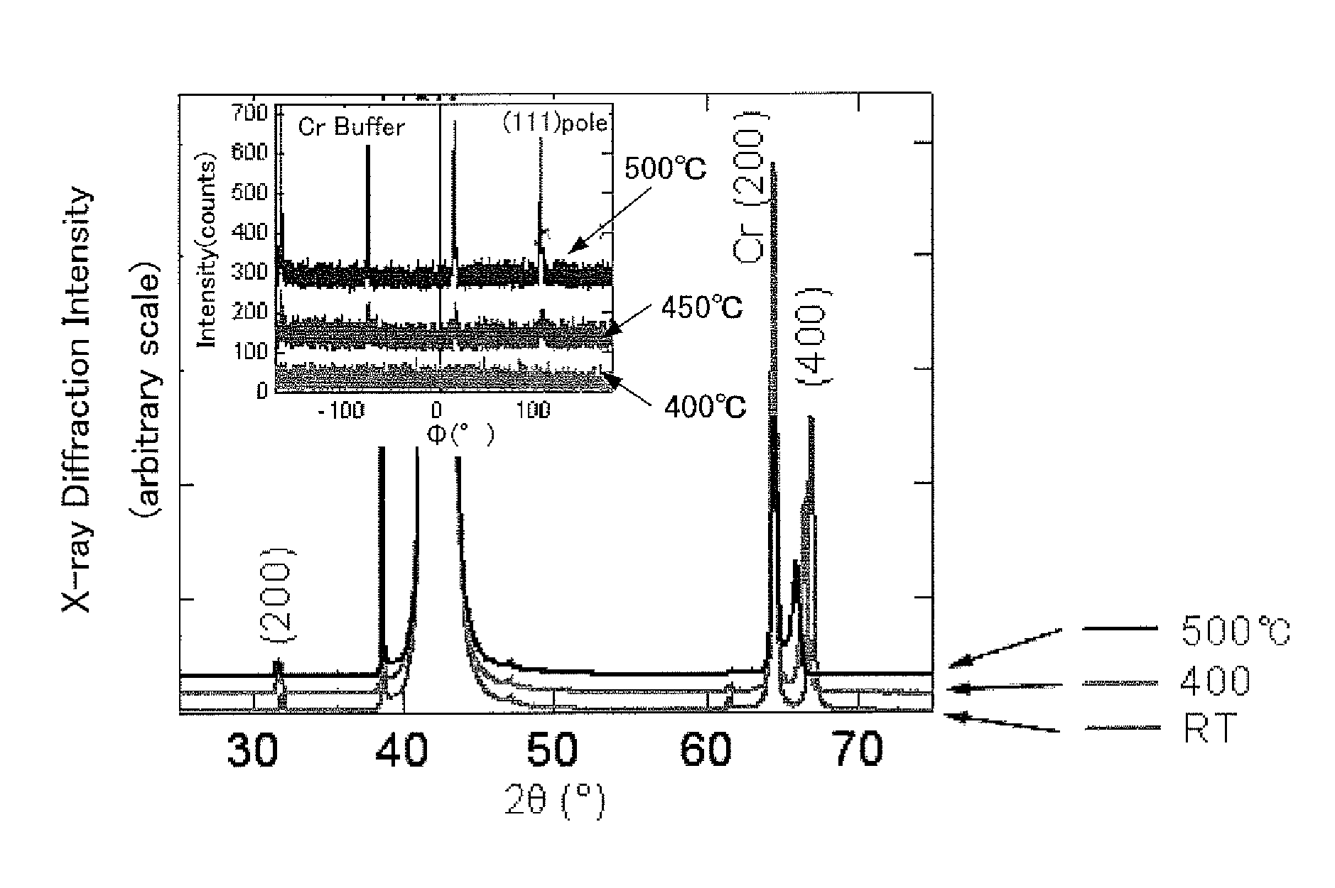
[0102]With the use of a high-frequency magnetron sputtering system, a thin film 3 of Co2Fe(Si0.5Al0.5) having a thickness of 100 nm was fabricated on a substrate 2 of MgO (001) and thereafter was heat-treated at a temperature up to 600° C. maximum.

[0103]FIG. 9 illustrates results of measurement on X-ray diffraction of the Co2Fe(Si0.5Al0.5) thin film 3 of Example 1. In FIG. 9, the ordinate axis represents the X-ray diffraction intensity (in arbitrary scale) and the abscissa axis represents the angle (in °), namely an angle corresponding to twice the angle of incidence θ of the X-ray on the atomic plane. FIG. 9 indicates a specimen having the Co2Fe(Si0.5Al0.5) thin film 3 deposited at room temperature and specimens having the depositions and then heat-treated at 500° C. and 600° C., respectively. As is apparent from FIG. 9, it is seen that the Co2Fe(Si0.5Al0.5) thin film 3 has a (001) orientation and is epitaxial...

example 2

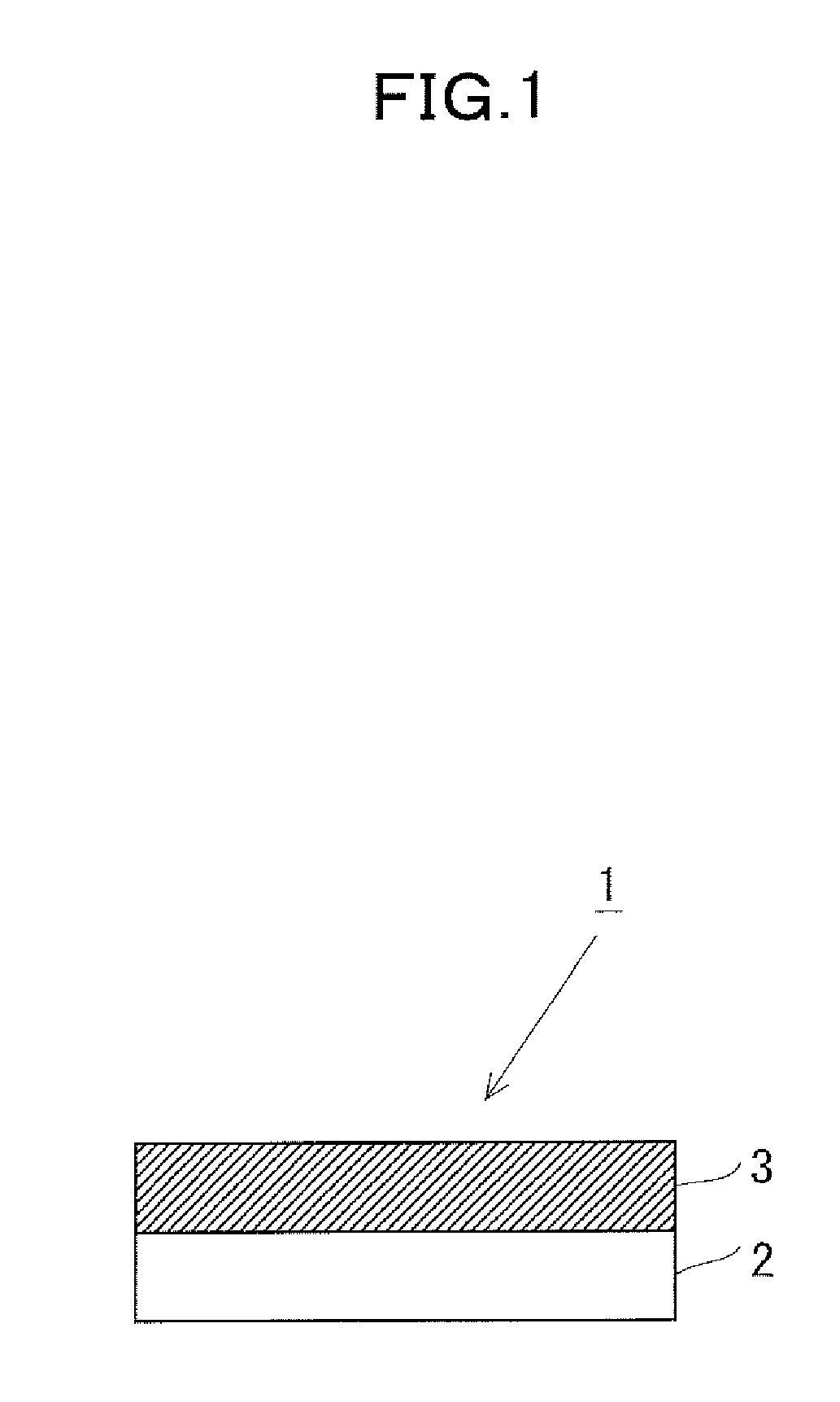
[0106]A Co2Fe(Si0.5Al0.5) thin films 3 of 100 nm thickness was fabricated in the same manner as in Example 1 except the use of a buffer layer 4 consisting of Cr. Afterwards it was heat-treated at temperature up to 600° C. maximum.

[0107]FIG. 10 illustrates results of measurement on X-ray diffraction of the Co2Fe(Si0.5Al0.5) thin film 3 of Example 2. The ordinate and the abscissa axes are same as in FIG. 9. FIG. 10 indicates a specimen having the Co2Fe(Si0.5Al0.5) thin film 3 deposited at room temperature and specimens having the depositions and then heat-treated at 400° C. and 500° C., respectively.

[0108]As is apparent from FIG. 10, it is seen that the Co2Fe(Si0.5Al0.5) thin film 3 fabricated in Example 2 has had a (001) orientation since before the heat treatment and the Cr buffer layer used improves the (001) orientation.

[0109]The inserted graph in FIG. 10 illustrates X-ray diffraction patterns of the specimens having the Co2Fe(Si0.5Al0.5) thin films 3 formed at room temperature an...

example 3

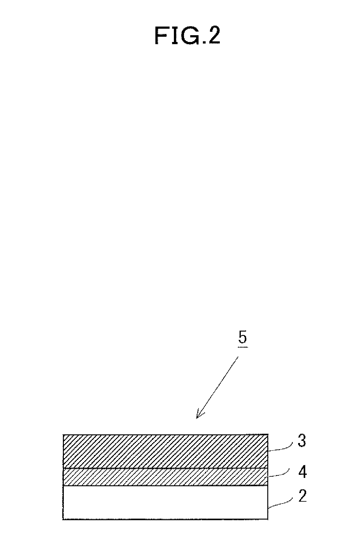
[0112]As Example 3, a tunneling magnetoresistance effect device (MTJ) 15 of spin valve type as shown in FIG. 5 was fabricated.

[0113]First, a Cr buffer layer 4 of 40 nm and a Co2Fe(Si0.5Al0.5) thin film 3 of 30 nm as a ferromagnetic free layer on the buffer layer 4 were deposited on a substrate 2 of MgO (001) by using the magnetron sputtering system. The Co2Fe(Si0.5Al0.5) thin film 3 after deposition was heat-treated at 400° C. to improve its crystal quality. The heat-treated Co2Fe(Si0.5Al0.5) thin film 3 had a B2 structure.

[0114]Subsequently, 1.2 nm of AlOx layer as a tunneling insulator layer 11, 3 nm of CoFe layer as a ferromagnetic pinned layer 12, 10 nm of IrMn layer as an antiferromagnetic layer 13 having a role to pin spin of the CoFe layer and 5 nm of Ta layer as an electrode layer 14 performing roles also as a protective layer and further for becoming mask in micro-fabrication were successively formed by deposition in this order. When the CoFe pinned layer 12 is deposited, h...


PUM

PropertyMeasurementUnit
resistivityaaaaaaaaaa
temperatureaaaaaaaaaa

Abstract

A magnetic thin film being ferromagnetic and exhibiting large spin polarization at room temperature is provided that comprises a substrate (2) and a Co2Fe(Si1-xAlx) thin film (3) formed on the substrate (2) where 0<x<1 and wherein the Co2Fe(Si1-xAlx) thin film (3) has a L21 or a B2 structure. There may be interposed a buffer layer (4) between the substrate (2) and the Co2Fe(Si1-xAlx) thin film (3). A tunneling magnetoresistance effect device and giant magnetoresistance effect device using such a magnetic thin film exhibit large TMR and GMR at room temperature, with low electric current and under low magnetic field. Using such a magnetoresistance effect device, a magnetic device and a magnetic apparatus such as a magnetic sensor, a magnetic head or MRAM are provided.

Description

TECHNICAL FIELD[0001]The present invention relates to a magnetic thin film that has a large spin polarization and also to a magnetoresistance effect device and a magnetic device using the same.BACKGROUND ART[0002]In recent years, a giant magnetoresistance (GMR) effect device consisting of a multi-layered film of ferromagnetic layer / nonmagnetic metal layer and a ferromagnetic tunneling junction (MTJ) device comprised of ferromagnetic layer / insulating layer / ferromagnetic layer have been drawing attention as new magnetic field sensors and nonvolatile random access magnetic memory (MRAM) devices. As giant magnetoresistance effect devices there are known those of CIP (Current in Plane) structure in which an electric current is passed in a film plane and those of CPP (Current Perpendicular to the Plane) in which a current is passed in a direction perpendicular to a film plane. Principles of the giant magnetoresistance effect device reside in spin dependent scattering at an interface betwe...

Claims


Application Information

Patent Timeline
Patent Type & Authority Patents(United States)
IPC IPC(8): G11B5/127
CPCB82Y10/00B82Y25/00C22C19/07C30B23/02C30B29/52G01R33/093G11B5/3909G11B5/3929G11C11/16H01F10/1936H01F10/3254H01F10/3268H01L43/10G11B2005/3996G11C11/161H10N50/85
Inventor INOMATA, KOUICHIROTEZUKA, NOBUKI
Owner JAPAN SCI & TECH CORP
Why Eureka
Try Eureka