Layered semiconductor wafer with low warp and bow, and process for producing it

Inactive Publication Date: 2006-03-02
SILTRONIC AG
View PDF6 Cites 45 Cited by
  • Summary
  • Abstract
  • Description
  • Claims
  • Application Information

AI Technical Summary

Benefits of technology

[0034] Another advantage of the invention is that the required changes to the heat treatment of the SOI wafer are simple to implement and have no harmful side effects on other important parameters of the finished SOI wafer.
[0035] The prior art has not disclosed a valid model which takes into account all the variables influencing the mechanical properties, in particular the deformation resistance of silicon wafers, simultaneously. This applies to an even greater extent in particular to semiconductor wafers with a layer structure which are produced by transferring a silicon layer and comprise a carrier wafer, an electrically insulating layer and a semiconductor layer.
[0036] The SOI wafers referred to have a specific thermal history behind them, leading to a specific BMD formation. FIG. 1 shows a typical BMD distribution in prior art SOI wafer of this type. The distribution is highly inhomogeneous, with a relatively low BMD density in the vicinity of the wafer back surface 3 but a BMD density which is higher by a multiple in the vicinity of the wafer front surface 1. The wafer front surface bears the thin film of silicon which is intended for the fabrication of electronic components. Overall, the BMD density decreases from the wafer front surface 1 to the center of the wafer 2 and then decreases further toward the wafer back surface 3. By

Problems solved by technology

However, SOI wafers which are produced by this process have the drawback of being deformed during this heat treatment, as well as during subsequent heat treatments associated with the fabrication of electronic components.
This deformation can lead to serious complications in the fabrication of electronic components.
If the wafer is deformed, it cannot be completely “sucked” onto the vacuum wafer holder, with the result that the surface is not planar during exposure.
In this case, sharply defined imaging of the mask pattern on the surface is not possible in all regions of the SOI wafer.
Moreover, this can lead to a lateral offset in the mask pattern transferred to the SOI wafer, with the result that adjacent c

Method used


Image

  • Layered semiconductor wafer with low warp and bow, and process for producing it
  • Layered semiconductor wafer with low warp and bow, and process for producing it
  • Layered semiconductor wafer with low warp and bow, and process for producing it

Examples


example 1a

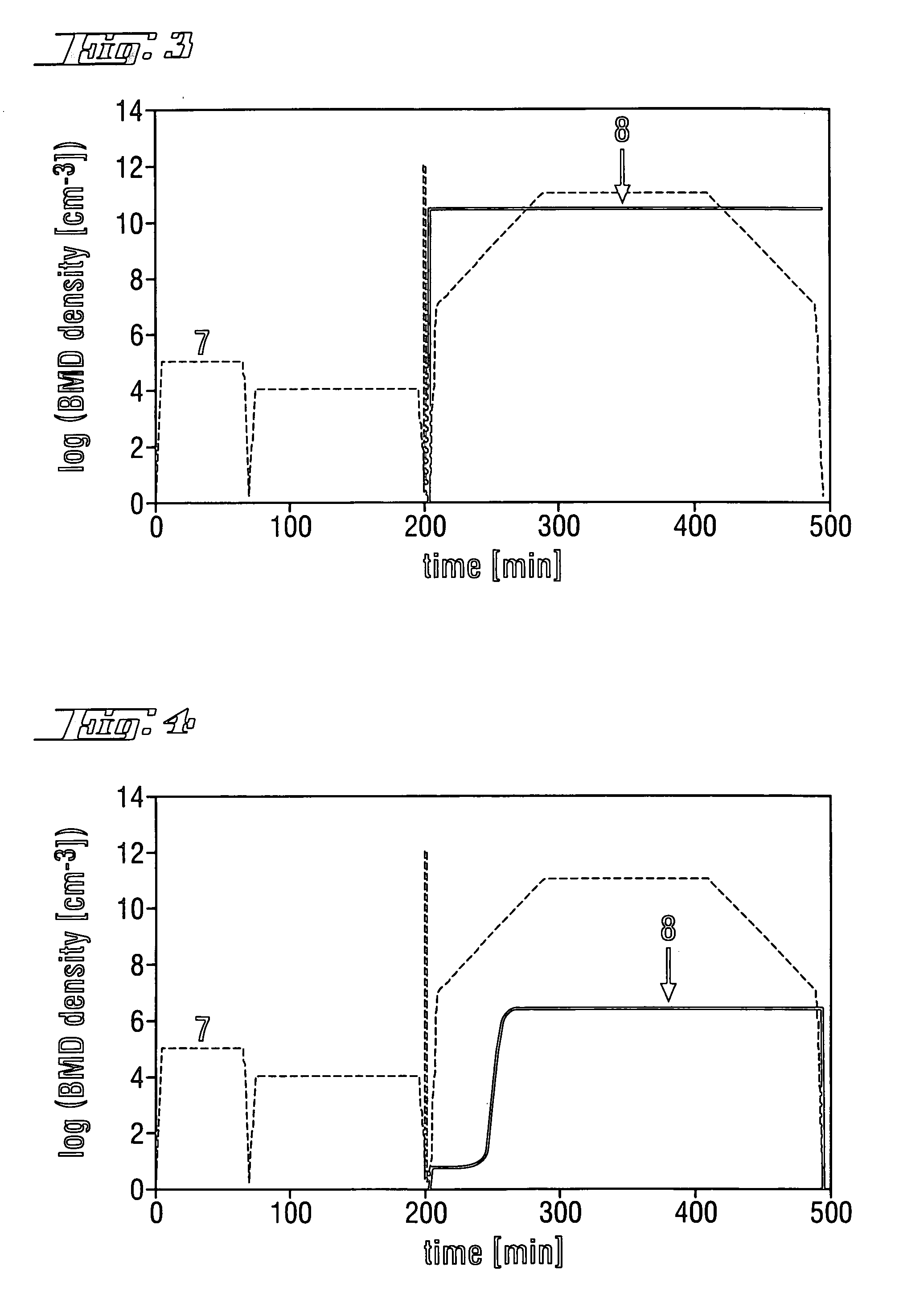
[0042] The RTA treatment was carried out in a nitrogen atmosphere in accordance with the first process according to the invention. The RTA treatment was carried out in a single stage at a heating rate of 100° C. / s to 1,200° C. The SOI wafer was then held at this temperature for 10 s and then cooled to room temperature at a cooling rate of 15° C. / s.

example 1b

[0043] The RTA treatment was carried out in a nitrogen atmosphere in accordance with the first process according to the invention. The RTA treatment was carried out in a single stage at a heating rate of 100° C. / s to 1,200° C. The SOI wafer was then held at this temperature for 10 s and then cooled to room temperature at a cooling rate of 5° C. / s.

example 2a

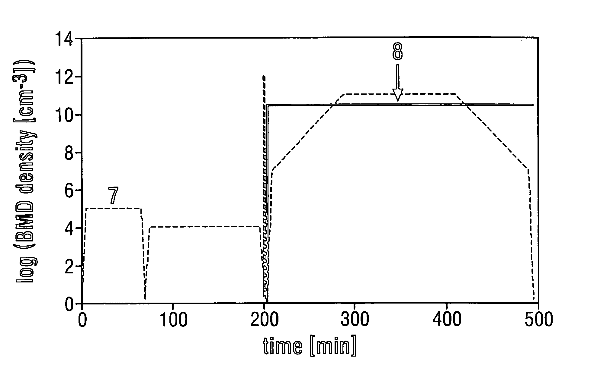
[0044] The RTA treatment was carried out in two stages in a nitrogen atmosphere in accordance with the second process according to the invention. The RTA treatment was carried out at a heating rate of 100° C. / s to 1,200° C. The SOI wafer was then held at this temperature for 10 s and then cooled to 1,000° C. at a cooling rate of 100° C. / s. The SOI wafer was then held at 1,000° C. for 90 s before being cooled to room temperature at a cooling rate of 100° C. / s.


PUM


Abstract

Semiconductor wafers with a diameter of at least 200 mm comprise a silicon carrier wafer, an electrically insulating layer and a semiconductor layer located thereon, the semiconductor wafer having been produced by means of a layer transfer process comprising at least one RTA step, wherein the semiconductor wafer has a warp of less than 30 μm, a DeltaWarp of less than 30 μm, a bow of less than 10 μm and a DeltaBow of less than 10 μm. Processes for the production of a semiconductor wafer of this type require specific heat treatment regimens.

Description

BACKGROUND OF THE INVENTION [0001] 1 Field of the Invention [0002] The invention relates to a semiconductor wafer with a diameter of at least 200 mm produced by a layer transfer process including at least one RTA step, and comprising a carrier wafer of silicon, an electrically insulating layer, and a semiconductor layer located thereon, the semiconductor wafer having low warp and bow, both in the unprocessed state and after any desired component fabrication process. Moreover, the invention relates to a process for producing such wafers. [0003] 2. Background Art [0004] SOI (silicon on insulator) wafers are generally produced by transferring a silicon layer from a donor wafer to a carrier wafer, also known as a handle wafer or a base wafer. Processes for producing SOI wafers by transferring a silicon layer (layer transfer) are described, for example, in EP533551A1, WO98 / 52216A1, and WO03 / 003430A2. SOI wafers comprise a carrier wafer and a single-crystal silicon covering layer, also kn...

Claims


Application Information

Patent Timeline
IPC IPC(8): H01L21/30
CPCH01L21/2007H01L21/20H01L27/12
Inventor BLIETZ, MARKUSHOELZL, ROBERTWAHLICH, REINHOLDHUBER, ANDREAS
Owner SILTRONIC AG
Why Eureka
Try Eureka