Circuit analysis method and circuit analysis apparatus

a circuit analysis and circuit analysis technology, applied in the field of circuit analysis methods and circuit analysis apparatus, can solve the problems of reducing affecting the accuracy of circuit analysis, so as to reduce the calculation of simulation, the effect of short time and high accuracy

Inactive Publication Date: 2006-03-02
FUJITSU LTD
View PDF32 Cites 19 Cited by
  • Summary
  • Abstract
  • Description
  • Claims
  • Application Information

AI Technical Summary

Benefits of technology

[0016] According to another preferable example in one aspect of the invention, first, a first parameter indicating a relationship between noise and jitter of the first clock caused by the noise is extracted. Next, jitter is generated in the first clock according to the first parameter to give jitter to the second discrete time model. Timing of a sampling edge of the first clock having the jitter and an effective signal value of a signal that is input to and output from the clock synchronous circuit at this timing are calculated by using the second discrete time model. An accurate simulation can be performed with not only waveform distortion of a signal input to/output from the clock synchronous circuit but also jitter of the first clock taken into consideration, so that it is possible to execute simulation with even higher accuracy in a short time.
[0017] According to another preferable example in one aspect of the invention, the first parameter is extracted from a relationship between a difference in phase between periodic noise and activation timing of the first clock and jitter of the first clock caused by the periodic noise. The extracted first parameter is stored in a table. A simulation is feasible by simply storing the first parameters corresponding to noise in one cycle. Also, the simulation is feasible by just referring to the table or interpolating the first parameters stored in the table. This can further reduce the calculation for the simulation.
[0018] According to another preferable example in one aspect of the invention, first, a second parameter indicating a relationship between noise and jitter in a second clock caused by the noise is extracted. The second clock is a regeneration clock generated by a clock regeneration circuit that is included in a circuit as the simulation subject. Next, jitter is generated in the second clock according to the second parameter to give jitter to the second discrete time model. An effective signal value of the second clock having the jitter that is output from the clock regeneration circuit is calculated by using the second discrete time model. In general, since a first clock is supplied from outside the circuit as the simulation subject, only needed is calculation of how a sampling edge of the supplied first clock fluctuates. In contrast, in the clock regeneration circuit, jitter in the second clock gives influence on the timing of the next edge of the second clock. Separately calculating jitter of the first clock that is not fed back

Problems solved by technology

With increase in chip size, not only the speed of signal transmission between chips but also that between the elements and circuit blocks in a chip is becoming a major factor of restricting the chip performance.
As the speed of signal transmission between circuit blocks, chips, or cases increases, various problems relating signal quality arise, an example of which is attenuation of high-frequency components of a signal.
Signal attenuation causes distortion of the waveform

Method used


Image

  • Circuit analysis method and circuit analysis apparatus
  • Circuit analysis method and circuit analysis apparatus
  • Circuit analysis method and circuit analysis apparatus

Examples


first embodiment

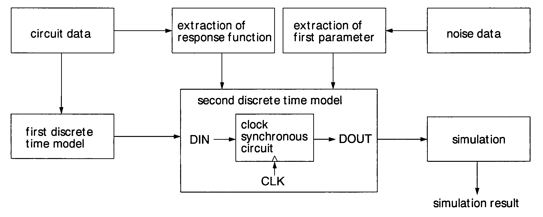
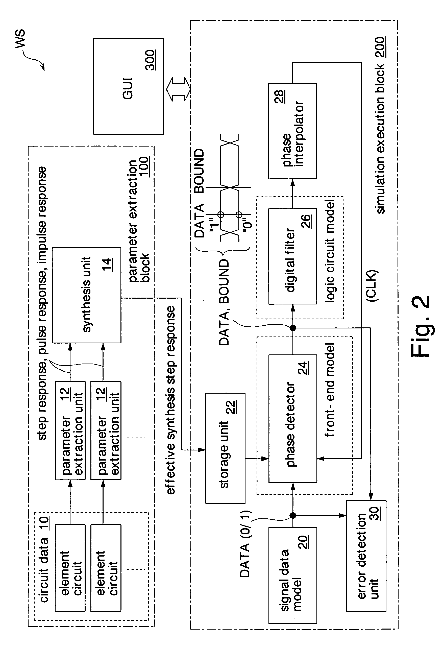
[0057]FIG. 2 shows the invention. Each element in FIG. 2 is a program that is executed by a workstation WS (computer) or data (file) that is accessed by the workstation WS. Each item of data is used by the workstation WS for executing a program or generated by the workstation WS's executing a program. Those programs and those items of data are stored on a recording medium such as a magnetic tape, an optical disc (MO or CD-ROM), a magnetic disk (hard disk drive), or the like. In general, a program is transferred to the hard disk drive of the workstation from the magnetic tape, optical disc, or the like, and stored in a hard disk drive of the workstation WS so as to be executable by the workstation WS.

[0058] In the following description, each element will be described as a component of the workstation WS.

[0059] The workstation WS has a first parameter extraction block 100, a simulation execution block 200, and a graphical user interface (GUI) 300. The workstation WS also has, in addi...

third embodiment

[0088] In addition to the functions of the third embodiment, this embodiment has a function for performing a simulation taking into consideration jitter (jitter of a regeneration clock) occurring in a clock regeneration circuit such as a VCO that generates a clock (second clock) regeneratively using a feedback loop.

[0089] Where a circuit block as a simulation subject has a clock synchronous circuit that receives a signal in synchronism with a clock (or a clock driving circuit such as a clock buffer that operates receiving a clock) and a clock regeneration circuit, jitter occurring in each of these circuits needs to be calculated separately. This is because the clock is supplied externally to the clock synchronous circuit (or clock driving circuit) and it is sufficient to calculate how edges of the supplied clock fluctuate, whereas in the clock regeneration circuit jitter occurring at a certain clock edge influences the position of the next clock edge. Therefore, whereas for the cloc...


PUM


Abstract

A step response of a clock synchronous circuit including a bandwidth restriction effect of a transmission path is extracted from circuit data on a simulation subject. A second discrete time model is generated by applying the response function to a first discrete time model generated from the circuit data. Using the second discrete time model, clock edge timing and an effective signal value of a signal input to/output from the clock synchronous circuit at this timing are calculated for simulation execution. Analogically accurate simulation of a circuit operation around a sampling edge of a clock enables precise simulation with a minimum calculation in a short time. Accordingly, the invention can provide an accurate simulation method for accurately modeling an analog operation of a signal transmission circuit that inputs and outputs a high-speed signal, to calculate in a short time.

Description

CROSS REFERENCE TO RELATED APPLICATION [0001] This application is based upon and claims the benefit of priority from Japanese Patent Application No. 2004-250274, filed on Aug. 30, 2004, the entire contents of which are incorporated herein by reference. BACKGROUND OF THE INVENTION [0002] 1. Field of the Invention [0003] The present invention relates to a technique for performing, at high speed, signal transmission between LSI chips, elements and circuit blocks in an LSI chip, boards, or cases. In particular, the invention relates to a circuit analysis method for designing a circuit that is used for such a technique. [0004] 2. Description of the Related Art [0005] The performance of components of data processing apparatus such as computers has been improving rapidly with the development of LSIs (semiconductor integrated circuits). For example, the performance of SRAMs, DRAMs, processors, and switching LSIs continues to improve year by year. To enhance the performance of systems accord...

Claims


Application Information

Patent Timeline
IPC IPC(8): G06F17/50
CPCG06F17/5036G06F30/367
Inventor TAMURA, HIROTAKAYAMAGUCHI, HISAKATSUIERSSEL, MARCUS VAN
Owner FUJITSU LTD
Why Eureka
Try Eureka