Nitride based hetero-junction field effect transistor

Inactive Publication Date: 2006-03-09
SAMSUNG ELECTRO MECHANICS CO LTD
View PDF13 Cites 25 Cited by
  • Summary
  • Abstract
  • Description
  • Claims
  • Application Information

AI Technical Summary

Benefits of technology

[0014] The present invention has been made in view of the above problems, and it is an object of the present invention to provide a nitride based hetero-junction field effect transistor, which is

Problems solved by technology

As a result, there are problems of a high carrier concentration due to the defects without doping impurities, and of difficulty to provide high carrier mobility.
However, even though the crystallinity of the GaN layer is enhanced by way of a secondary high temperature growth, it is difficult to substantially enhance the crystallinity, since the GaN layer grown by way of the secondary h

Method used


Image

  • Nitride based hetero-junction field effect transistor
  • Nitride based hetero-junction field effect transistor
  • Nitride based hetero-junction field effect transistor

Examples


example

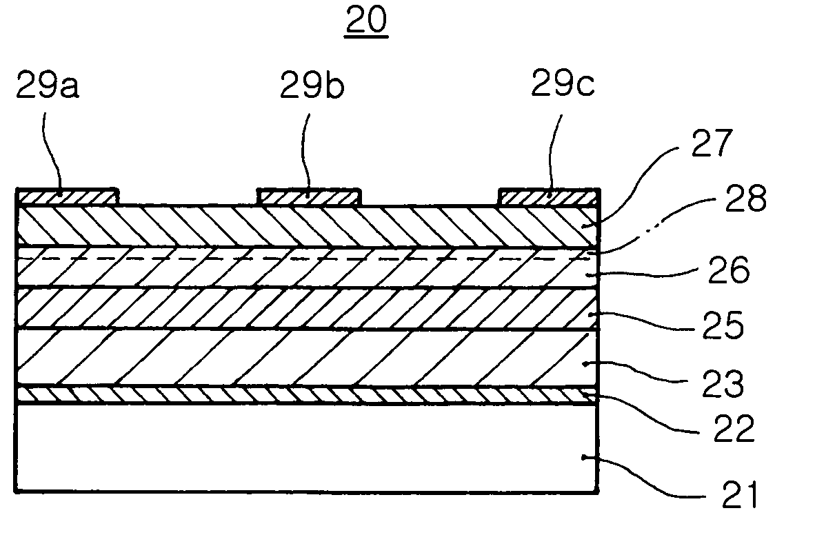
[0042] This example is provided to verify enhancement of crystallinity of an undoped GaN layer, which forms a hetero-junction with an AlGaN layer in a hetero-junction field effect transistor according to the present invention, reduction of carrier concentration (the concentration of the carriers generated not by impurity doping but by defects), and an increase of the mobility due to the enhanced crystallinity.

[0043] First, in the case of Sample A, after growing a GaN layer at a low temperature as a buffer layer on a sapphire substrate, a high resistance GaN layer having a thickness of about 2 μm is grown under the condition wherein the high resistance GaN layer is primarily grown at a temperature of about 900° C. for about 1 minute, and secondarily grown at a temperature of about 1,050° C. for about 40 minutes after being grown for two minutes at a temperature increasing from 900° C. to 1,050° C. With the same method, other Samples B, C, and D are prepared for the test.

[0044] In t...


PUM


Abstract

A nitride based hetero-junction field effect transistor comprises a high resistance nitride semiconductor layer formed on a substrate, an Al-doped GaN layer formed on the high resistance nitride semiconductor layer and having an Al content of 0.1˜1%, an undoped GaN layer formed on the Al-doped GaN layer, and an AlGaN layer formed on the undoped GaN layer such that a two-dimensional electron gas (2DEG) layer is formed at an interface of the undoped GaN layer. With the Al-doped GaN layer and the undoped GaN layer grown on the high resistance GaN layer having low crystallinity, crystallinity of the GaN layer is enhanced, and thus electrical characteristics of DC and RE of an HEET device are remarkably improved due to enhanced carrier mobility.

Description

RELATED APPLICATIONS [0001] The present application is based on, and claims priority from, Korean Application Number 2004-71616, filed Sep. 8, 2004, the disclosure of which is incorporated by reference herein in its entirety. BACKGROUND OF THE INVENTION [0002] 1. Field of the Invention [0003] The present invention relates to a hetero-junction field effect transistor, and more particularly, to a high-power nitride based hetero-junction field effect transistor having enhanced high frequency characteristics. [0004] 2. Description of the Related Art [0005] Recently, a hetero-junction field effect transistor has been made of a nitride based-compound semiconductor to satisfy requirements for high frequency and high power electrical devices. Generally, since the nitride semiconductor has a wider band gap energy, a higher thermal / chemical stability, and a higher electron saturation velocity, compared with a typical semiconductor material, it has been widely applied not only to photo devices...

Claims


Application Information

Patent Timeline
IPC IPC(8): H01L29/739
CPCH01L29/7787H01L29/2003H01L29/66431H01L29/778H01L2924/1033H01L2924/10344
Inventor LEE, JAE HOONLEE, JUNG HEE
Owner SAMSUNG ELECTRO MECHANICS CO LTD
Why Eureka
Try Eureka