Solid-state image sensor
a solid-state image and sensor technology, applied in the field of solid-state image sensors, can solve the problems of disadvantageous increase of signal voltage, disadvantageous reduction of etc., and achieve the effect of improving the detection sensitivity of output signals
- Summary
- Abstract
- Description
- Claims
- Application Information
AI Technical Summary
Benefits of technology
Problems solved by technology
Method used
Image

Examples
first embodiment
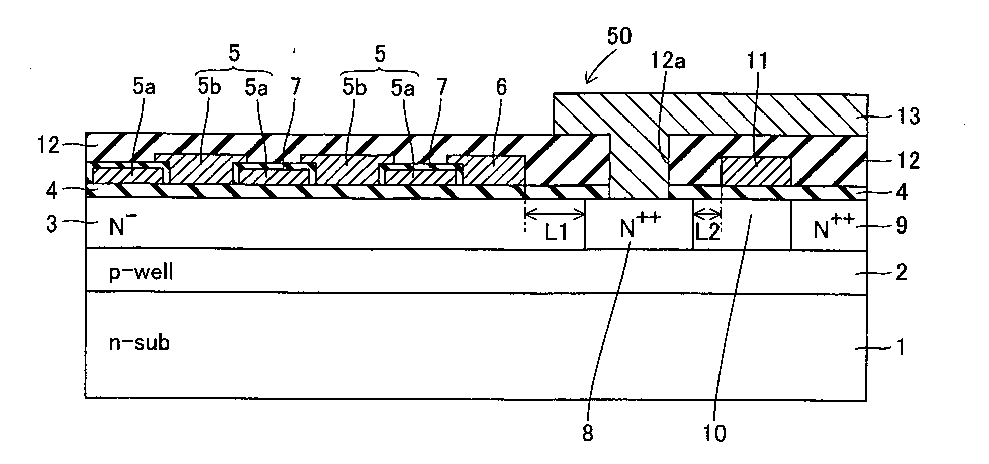
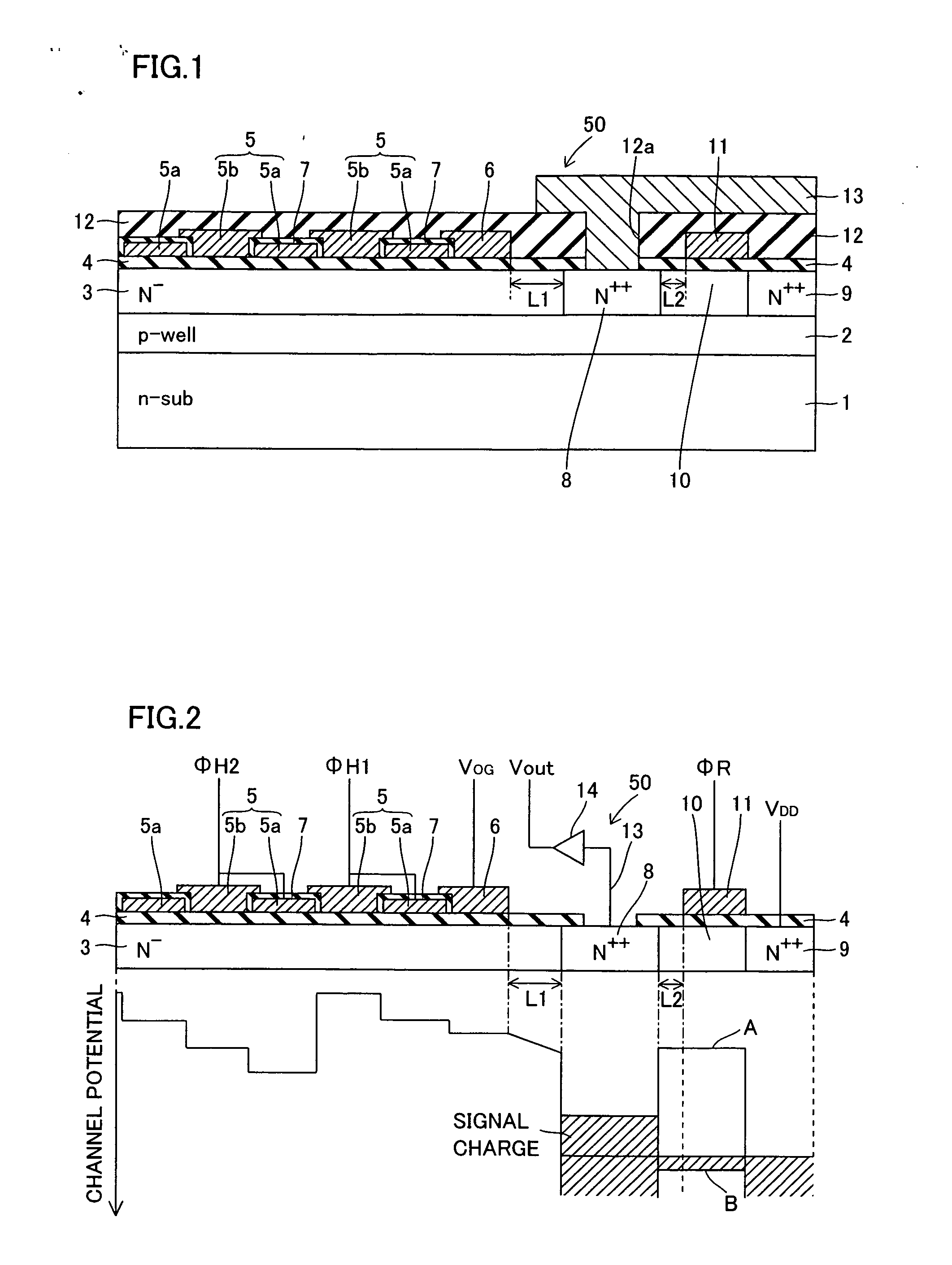
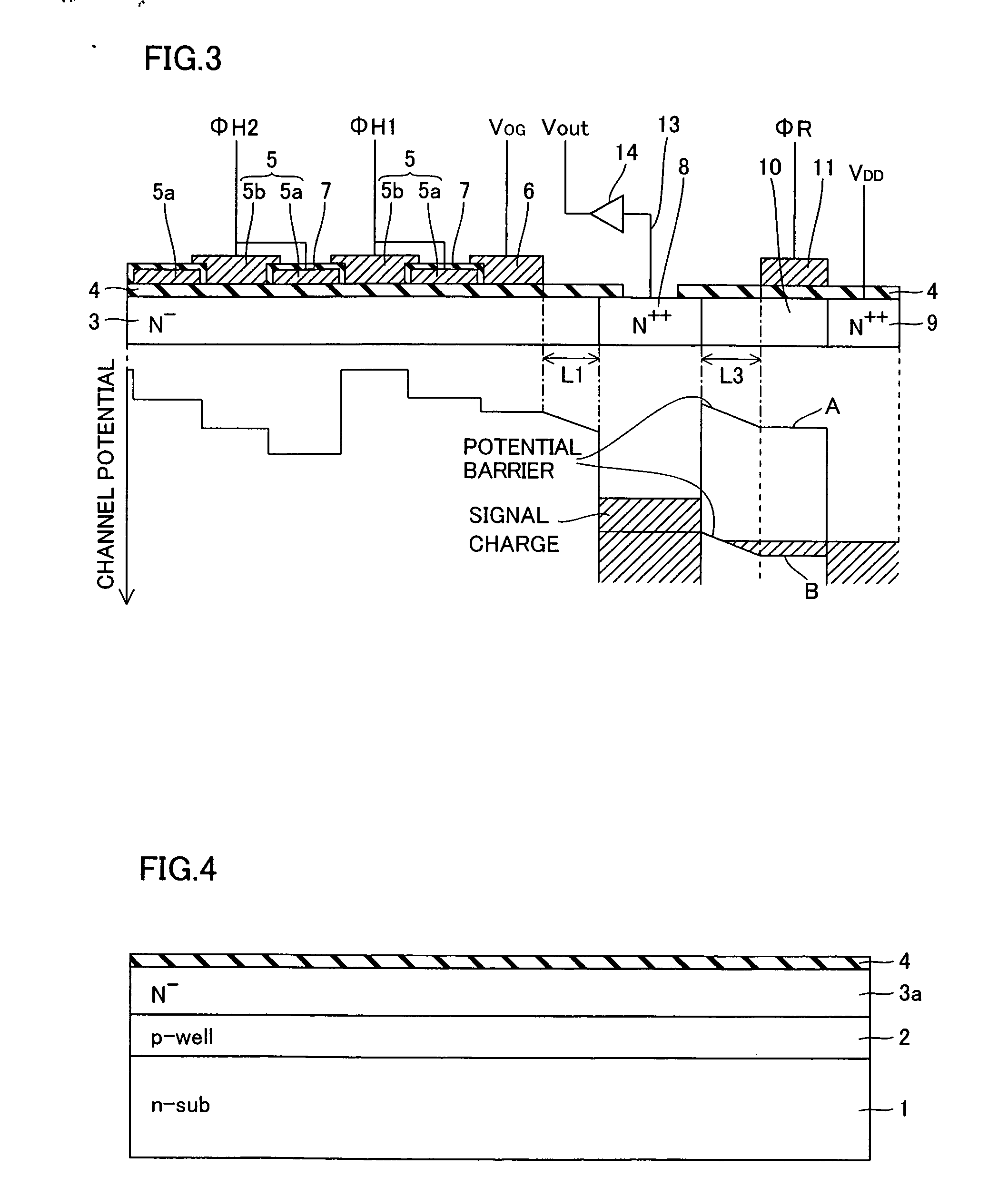
[0052] The structure of a solid-state image sensor according to a first embodiment of the present invention is described with reference to FIGS. 1 and 2.
[0053] The solid-state image sensor according to the first embodiment comprises an n-type silicon substrate 1, as shown in FIG. 1. This n-type silicon substrate 1 is an example of the “semiconductor substrate” in the present invention. A p-type well region 2 is formed with a depth of at least about 0.5 μm and not more than 4 μm from the upper surface of the n-type silicon substrate 1. An N−-type transfer channel region 3 having an impurity concentration of about 1016 cm−3 is formed on the surface of the p-type well region 2. This transfer channel region 3 is an example of the “charge storage part” in the present invention. The transfer channel region 3 is formed up to a depth of about 0.5 μm from the upper surface of the n-type silicon substrate 1. The transfer channel region 3 has a function of storing and transferring signal char...
second embodiment
[0075] The structure of a solid-state image sensor according to a second embodiment of the present invention is now described with reference to FIGS. 9 and 10.
[0076] In the solid-state image sensor according to the second embodiment shown in FIG. 9, an N+-type impurity region 16 having an impurity concentration of about 1018 cm3 is formed on a region of an n-type silicon substrate 1 located between an N++-type floating diffusion region 8 and an output gate electrode 6, dissimilarly to the aforementioned solid-state image sensor according to the first embodiment. This N+-type impurity region 16 is an example of the “second impurity region” in the present invention. In other words, the N+-type impurity region 16 having the impurity concentration (about 1018 cm−3) higher than the impurity concentration (about 1016 cm−3) of an N—type transfer channel region 3 and lower than the impurity concentration (about 1020 cm−3) of the N++-type floating diffusion region 8 is formed on the region ...
third embodiment
[0089] The structure of a CMOS image sensor according to a third embodiment of the present invention is now described with reference to FIGS. 18 and 19.
[0090] In the CMOS image sensor according to the third embodiment, an N−-type photodiode layer 23 is formed on the surface of a p-type well region 2 of an n-type silicon substrate 1 in place of the transfer channel region 3 shown in FIG. 1, dissimilarly to the aforementioned solid-state image sensor according to the first embodiment. This photodiode layer 23 is an example of the “photoelectric conversion part” or the “charge storage part” in the present invention. The photodiode layer 23 has a function of generating signal charges by receiving light and photoelectrically converting the same and storing the generated signal charges. A plurality of such photodiode layers 23 are formed on the surface of the p-type well region 2 in the form of a matrix. According to the third embodiment, an output part 60 is provided every photodiode la...
PUM
 Abstract
Description
Claims
Application Information
 - R&D
- Intellectual Property
- Life Sciences
- Materials
- Tech Scout
- Unparalleled Data Quality
- Higher Quality Content
- 60% Fewer Hallucinations
Browse by: Latest US Patents, China's latest patents, Technical Efficacy Thesaurus, Application Domain, Technology Topic, Popular Technical Reports.
© 2025 PatSnap. All rights reserved.Legal|Privacy policy|Modern Slavery Act Transparency Statement|Sitemap|About US| Contact US: help@patsnap.com