[0011] An
advantage of the invention is that it provides a transflective color liquid
crystal display device using vertical-alignment-type liquid crystal, capable of reliably regulating directions in which liquid crystal molecules are inclined in a reflective display region and of achieving display having high brightness and a wider viewing angle both in a reflective mode and in a transmissive mode. Another
advantage of the invention is that it provides an electronic apparatus including the liquid
crystal display device therein, so that the electronic apparatus has a high level of
visibility.
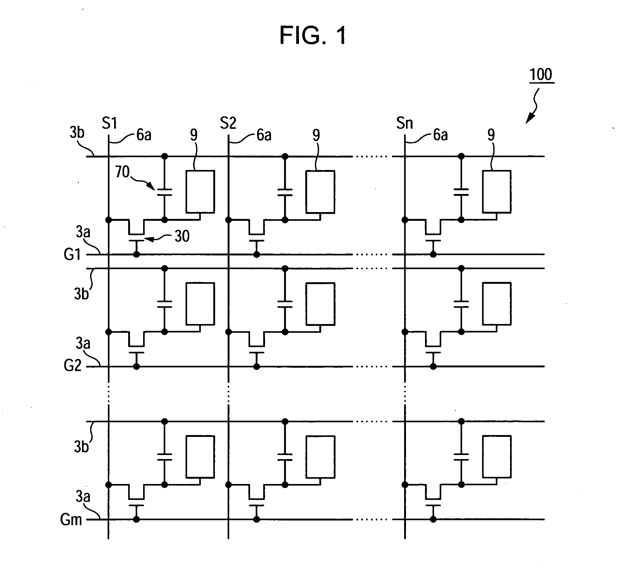
[0012] According to an aspect of the invention, a liquid crystal
display device includes a pair of substrates; a liquid crystal layer that is formed between the pair of substrates, and that is composed of liquid crystal having negative
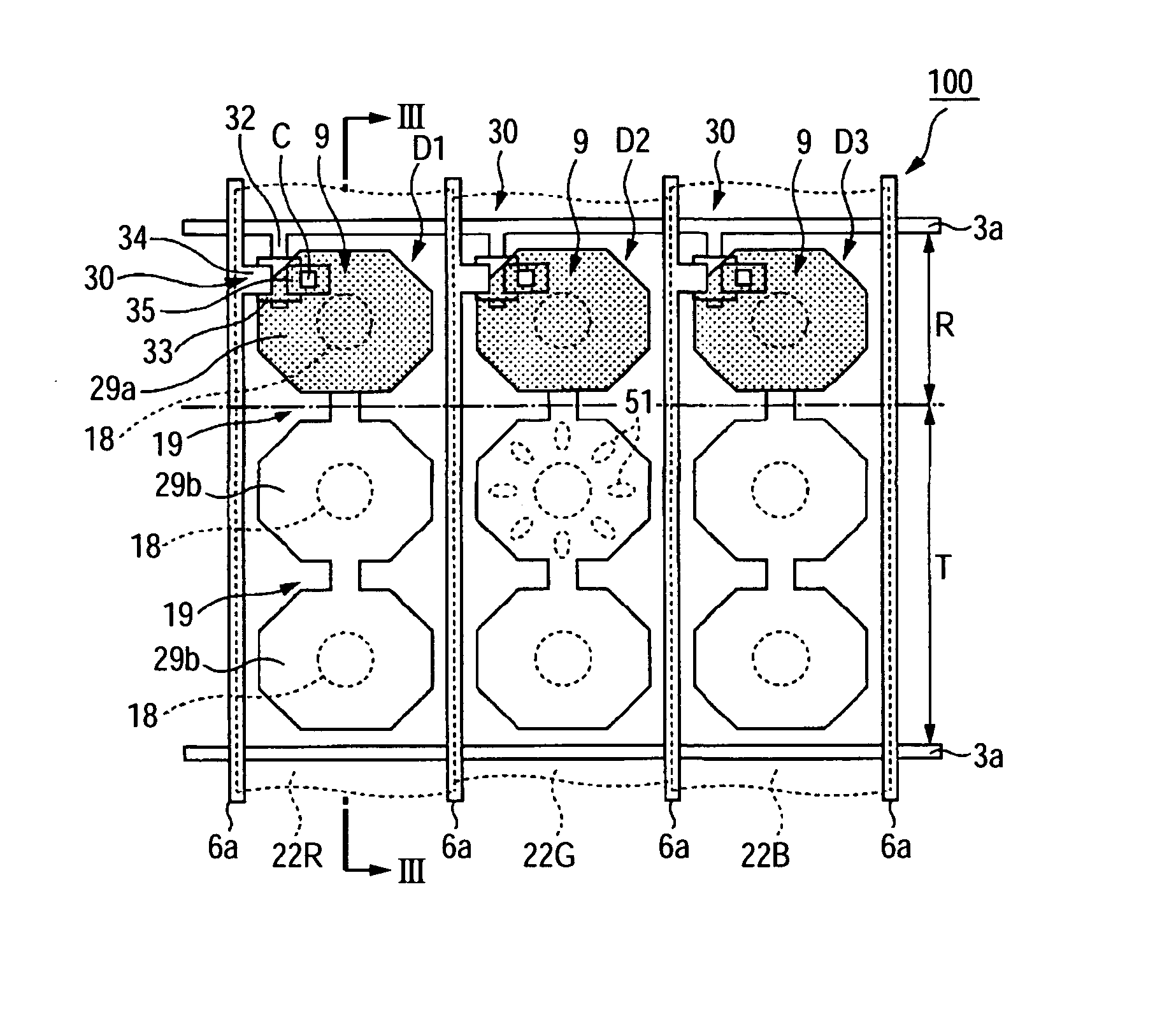
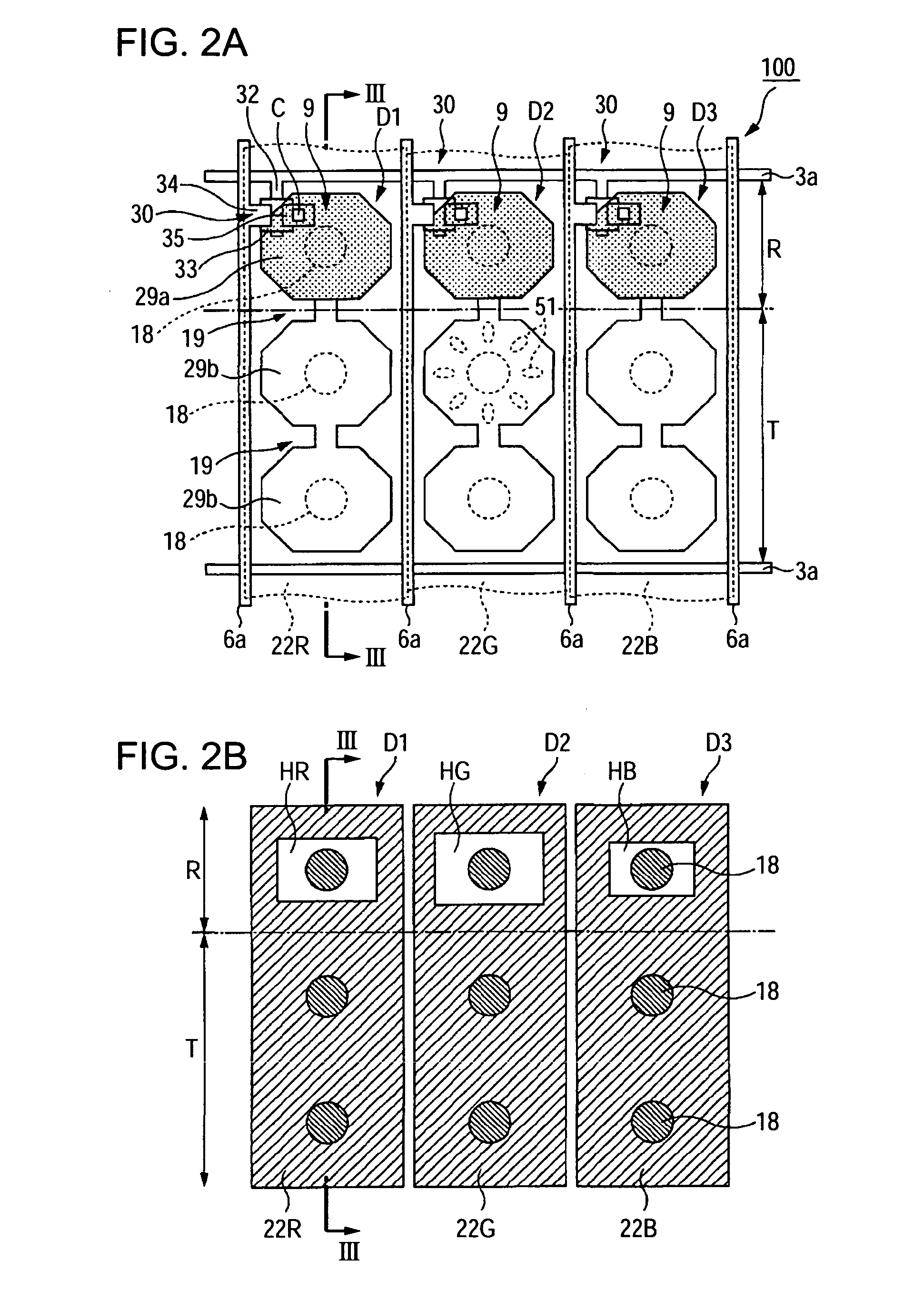
dielectric anisotropy, the liquid crystal being vertically aligned in an initial state; dot regions each having a transmissive display region and a reflective display region; a liquid-crystal-layer-thickness adjusting layer that is provided between the liquid crystal layer and at least one of the pair of substrates to make the thickness of the liquid crystal layer in the reflective display region smaller than the thickness of the liquid crystal layer in the transmissive display region; a color filter layer that includes plural types of colored
layers having different colors corresponding to the respective dot regions, and that is provided on at least one of the pair of substrates; and alignment regulators that are provided on an inner surface of at least one of the pair of substrates to regulate the alignment of the liquid crystal in the reflective display regions. In the liquid crystal display device, a colored region having the colored layer formed therein and a non-colored region not having the colored layer formed therein are provided in a portion of the colored layer that is arranged in the reflective display region, and the alignment regulators are arranged so as to overlap the non-colored regions of the color filter layer in the reflective display regions in plan view. In the liquid crystal display device of the invention, it is preferable that electrodes for driving the liquid crystal be provided on inner surfaces of the pair of substrates, respectively, and that each alignment
regulator be composed of an
electrode slit (for example, a slit-shaped opening) formed by
cutting out a portion of the
electrode or a
dielectric projection provided on the
electrode.
[0013] The liquid crystal display device of the invention has a structure for properly controlling the alignment direction of liquid crystal molecules by incorporating liquid crystal of a
vertical alignment mode into a
transflective liquid crystal display device and by additionally providing a liquid-crystal-layer-thickness adjusting layer for making retardation in the reflective display region substantially equal to that in the transmissive display region (that is, by additionally providing a multi-gap structure). Further, the liquid crystal display device of the invention includes the color filter layer having a plurality of colored
layers corresponding to the respective dot regions, which enables a color display. In the transflective color liquid crystal display device of the invention, light passes through the colored layer one time in the reflective mode, and it passes through the colored layer the two times in the transmissive mode to perform color display. In this case, when a light coloring material is used for the colored layer, regarding display in the reflective mode as important, it is difficult to obtain high-contrast display in the transmissive mode. On the contrary, when a deep coloring material is used for the colored layer, regarding display in the transmissive mode as important, reflected light has a deep color, which results in dark display. In order to solve these problems, the following two structures have been suggested: a structure in which different coloring materials are used for the reflective display region and the transmissive display region, respectively; and a structure in which non-colored regions (for example, openings) are formed in the colored layer of the reflective display region to perform color adjustment in reflective display. The liquid crystal display device of the invention adopts the latter structure.
[0014] In the invention, since alignment regulators, such as projections, are arranged in non-colored regions of the colored layer, it is possible to increase the thickness of the liquid crystal layer in a portion where the alignment
regulator is formed by the thickness of the colored layer in practice. That is, in a case in which projections are arranged in a region where the colored layer is formed, when the projections are formed in the reflective display region and the transmissive display region by the same process, and when the projections are formed with a height suitable for the transmissive display region, the height of the projection is excessively large in the reflective display region, which causes the leakage of light to occur in the vicinity of the projection, resulting in a reduction in contrast. On the other hand, when the projections are formed with a height suitable for the reflective display region, the height of the projection is excessively small in the transmissive display region, so that it is difficult to perform sufficient alignment control, which causes a spotted pattern to be generated due to
disclination. On the contrary, when the projections are arranged in the non-colored region of the colored layer so as to be buried in the colored layer, the height of the projection is decreased by a height corresponding to the buried portion, so that a gap from the top of the projection to a surface of the counter substrate is increased in practice. Therefore, good alignment control can be performed in the reflective display region where the gap is relatively narrow, as in the transmissive display region.
[0015] In the above-mentioned structure, it is preferable that one of the plural types of colored layers having a specific color be arranged such that the colored region thereof overlaps the alignment regulators in plan view, and that the colored layers having the other colors be arranged such that the non-colored regions thereof overlap the alignment regulators in plan view.
[0016] It has been known that a slight shift in color from white to yellow occurs in the color liquid crystal display device of a
vertical alignment mode when a
high voltage is applied, and the shift in color is a problem to be solved. This is caused by so-called chromatic dispersion in which a variation in the retardation of the liquid crystal layer is different for every color when a
voltage is applied. It is possible to reduce the variation in color to some extent by adjusting the spectrum of light emitted from, for example, a backlight, in transmissive display. However, since external light difficult to control is used in reflective display, the shift in color from white to yellow comes into a serious problem. Meanwhile, in a case in which the projections are used for controlling the directions in which the liquid crystal molecules are inclined, when a
voltage is applied, the distribution of an
electric field occurs in the plane in a place where the projection is present and in a place where the projection is absent, which causes the distribution of brightness to occur in the plane. When a
low voltage is applied, the region where the projection is formed does not transmit light. However, when a
high voltage is applied, the region where the projection is formed also contributes to bright display. The invention improves color reproducibility in the reflective mode by changing the relative position between the projection and the colored region in the reflective display region for every color, using the fact that the region where the projection is formed contributes to bright display when a high
voltage is applied. In the invention, the colored region is arranged so as to overlap, in plan view, the projection in a dot region having a color (for example, blue) whose shade is light when a
low voltage is applied or whose shade is deep when a high voltage is applied. In addition, the projections of dot regions having the other colors (for example, red and green) are arranged at positions corresponding to the non-colored regions so as not to overlap the colored regions in plan view. In this structure, when a
low voltage is applied, the liquid crystal molecules positioned around the projections hardly contribute to bright display. Therefore, the loss of light corresponding to the area of the projection occurs in the colored region arranged to overlap the projection, which results in dark display (light-colored display). Meanwhile, when a high voltage is applied, the liquid crystal molecules positioned around the projections also contribute to bright display. Therefore, the loss of light is reduced, resulting in bright display (deep-colored display). As such, according to the structure of the invention, a deep color tones down when a low voltage is applied, and a light color is enhanced when a high voltage is applied, which makes it possible to achieve display having a high degree of color reproducibility, regardless of an applied voltage.

