Multilayered printed circuit board

a printed circuit board and multi-layer technology, applied in the field of multi-layer printed circuit boards, can solve the problems of changing power supply and ground potential, affecting the operation of the circuit itself, so as to achieve the effect of effectively using a bypass capacitor and suppressing radiated nois

Inactive Publication Date: 2006-03-09
CANON KK
View PDF6 Cites 46 Cited by
  • Summary
  • Abstract
  • Description
  • Claims
  • Application Information

AI Technical Summary

Benefits of technology

[0014] The present invention suppresses radiated noise by effectively using a bypass capacitor with a simple arrangement in a printed circuit board that includes power supply wiring of a semiconductor integrated circuit extending through vias to the back face of the printed circuit board opposite to the face of the printed circuit board on which the semiconductor integrated circuit is provided, and that includes the bypass capacitor.
[0019] According to the present invention, the impedance between the inner-layer main power supply plane and the power supply terminal of the semiconductor integrated circuit is higher than the impedance between the bypass capacitor and the power supply terminal of the semiconductor integrated circuit. Thus, the amount of current flowing into the bypass capacitor increases and the radiated noise is suppressed. That is to say, the bypass capacitor can be effectively used.
[0020] In the present invention, the power supply patterns described above are installed in the printed circuit board. Thus, cost reduction can be achieved by preventing a repetition of prototyping due to the radiated noise and a malfunction of devices in product development, and by reducing anti-radiated noise components.

Problems solved by technology

However, on the other hand, higher integration and higher processing speed of a semiconductor integrated circuit cause changes in power supply and ground potential, radiated noise, or the like, which leads to serious problems, for example, an adverse effect on other electronic devices and malfunction of the circuit itself.
That is to say, a semiconductor integrated circuit requires a large current due to higher integration, and thus small inductance in a power supply pattern in a printed circuit board causes a large change in power supply voltage.
Moreover, radiated noise is caused by changes in power supply and ground potential of a semiconductor integrated circuit, a change in common mode voltage to which the changes in power supply and ground potential are converted on a printed circuit board, and the like.
A large portion of the area around such a semiconductor package is occupied by lead-out signal lines, and it is difficult to install the power supply wiring pattern disclosed in the document described above.
Accordingly, radiated noise is not effectively suppressed by the bypass capacitor 112.

Method used


Image

  • Multilayered printed circuit board
  • Multilayered printed circuit board
  • Multilayered printed circuit board

Examples


first embodiment

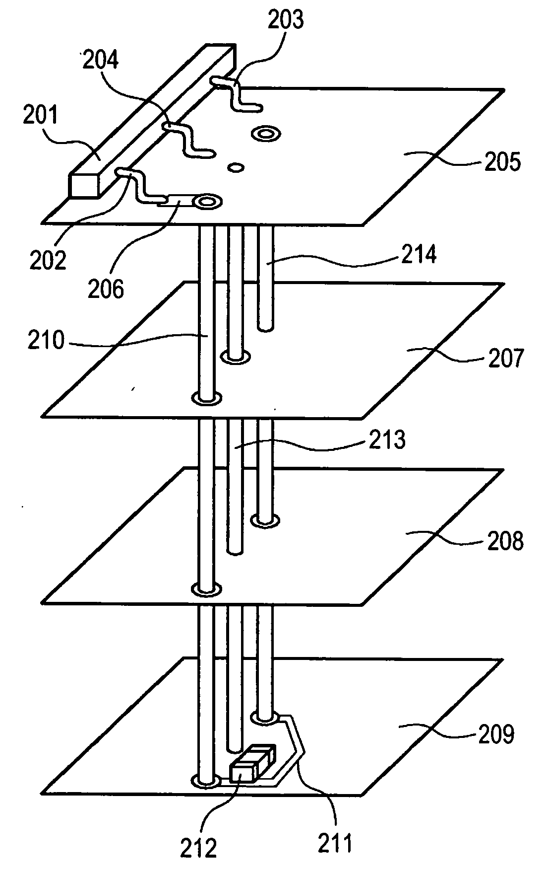
[0038]FIG. 1 is a schematic diagram showing a printed circuit board according to a first embodiment of the present invention.

[0039] In FIG. 1, the printed circuit board includes an IC 201 that generates noise, a power supply terminal 202 that supplies power to the IC 201, a ground terminal 203 that supplies a reference potential to the IC 201, and an I / O terminal 204 having a predetermined function for the IC 201. The printed circuit board further includes a first surface-layer conductor 205 on which the IC 201 is mounted, and first power supply wiring 206 installed in the first surface-layer conductor 205. The printed circuit board further includes an inner-layer main power supply plane 207 that constitutes a power supply system of the printed circuit board and that is disposed directly under the first surface-layer conductor 205, an inner-layer ground conductor 208, and a second surface-layer conductor 209 on a face of the printed circuit board opposite to a face of the printed c...

second embodiment

[0055]FIG. 5 is a schematic diagram showing a second embodiment according to the present invention. In FIG. 5, a printed circuit board includes an IC 601 that generates noise, a power supply terminal 602 that supplies power to the IC 601, a ground terminal 603 that supplies a reference potential to the IC 601, and an I / O terminal 604 having a predetermined function for the IC 601. The printed circuit board further includes a first surface-layer conductor 605 on which the IC 601 is mounted, and first power supply wiring 606 installed in the first surface-layer conductor 605. The printed circuit board further includes an inner-layer main power supply plane 607 that constitutes a power supply system of the printed circuit board and that is disposed directly under the first surface-layer conductor 605, an inner-layer ground conductor 608, and a second surface-layer conductor 609 on a face of the printed circuit board opposite to a face of the printed circuit board on which the first sur...

third embodiment

[0058]FIG. 6 is a sectional view showing the structure of a printed circuit board according to a third embodiment of the present invention. A power supply pin 702 of an IC 701 of the QFP type or small outline package (SOP) type is attached to first power supply wiring 706 provided on the printed circuit board by soldering. Second power supply wiring 711 for attaching a bypass capacitor 712 is provided on a second surface-layer conductor 709 that is provided on a face of the printed circuit board opposite to a face of the printed circuit board on which a first surface-layer conductor 705 is provided.

[0059] The printed circuit board includes four wiring layers having an insulating substrate 720. First to fourth layers are disposed in this order from the top. An inner-layer main power supply plane 707 is provided in the second layer, and an inner-layer ground plane 708 is provided in the third layer. A second power-supply via hole 714 with an inside diameter less than 0.4 mm connects ...


PUM


Abstract

A multilayered printed circuit board includes a first surface layer that includes a semiconductor integrated circuit, a second surface layer that includes a bypass capacitor and that is opposite to the first surface layer, a main power supply wiring layer, and a ground layer between the first and second surface layers. In the multilayered printed circuit board, one terminal of the bypass capacitor is connected to a midpoint of a wiring path from the main power supply wiring layer to a power supply terminal of the semiconductor integrated circuit, and an impedance of a first wiring path from the main power supply wiring layer to the terminal of the bypass capacitor is higher than an impedance of a second wiring path from the terminal of the bypass capacitor to the power supply terminal of the semiconductor integrated circuit.

Description

BACKGROUND OF THE INVENTION [0001] 1. Field of the Invention [0002] The present invention relates to multilayered printed circuit boards including semiconductor integrated circuits (IC / LSI) and bypass capacitors. [0003] 2. Description of the Related Art [0004] Recently, higher functionality has been required for electronic devices, and thus higher integration and higher processing speed of a semiconductor integrated circuit (IC / LSI), for example, an application specific integrated circuit (ASIC), mounted on a printed circuit board, have been developed to meet this requirement. [0005] However, on the other hand, higher integration and higher processing speed of a semiconductor integrated circuit cause changes in power supply and ground potential, radiated noise, or the like, which leads to serious problems, for example, an adverse effect on other electronic devices and malfunction of the circuit itself. That is to say, a semiconductor integrated circuit requires a large current due t...

Claims


Application Information

Patent Timeline
Patent Type & Authority Applications(United States)
IPC IPC(8): H05K7/08
CPCH05K1/0231H05K1/165H05K3/429H05K2201/10689H05K2201/0949H05K2201/10545H05K2201/09263
Inventor HAYASHI, SEIJIINAGAWA, HIDEHO
Owner CANON KK
Why Eureka
Try Eureka