
Semiconductor integrated circuit device

a technology of integrated circuits and semiconductors, applied in semiconductor devices, digital storage, instruments, etc., can solve the problems of destroying the symmetry of memory cells, unable or at least very difficult to microfabricate ultrafine layout patterns, and increasing the requirements for micro-patterning architectures

Inactive Publication Date: 2006-03-09
OSADA KENICHI +3
View PDF2 Cites 17 Cited by
  • Summary
  • Abstract
  • Description
  • Claims
  • Application Information

AI Technical Summary

Problems solved by technology

Unfortunately, the requirements for micro-patterning architectures have grown more rapidly than technological advance in the trend of shortening wavelengths in such equipment.
This makes it impossible, or at least very difficult, to microfabricate ultrafine layout patterns while disadvantageously serving as the cause of the destruction of the symmetry of memory cells.
Thus, the prior art suffers from the problem of the degradation of the symmetrization of the cell layout pattern, making the successful achievement of microfabrication architectures for higher integration densities difficult.

Method used


Image

  • Semiconductor integrated circuit device
  • Semiconductor integrated circuit device
  • Semiconductor integrated circuit device

Examples


embodiment 1

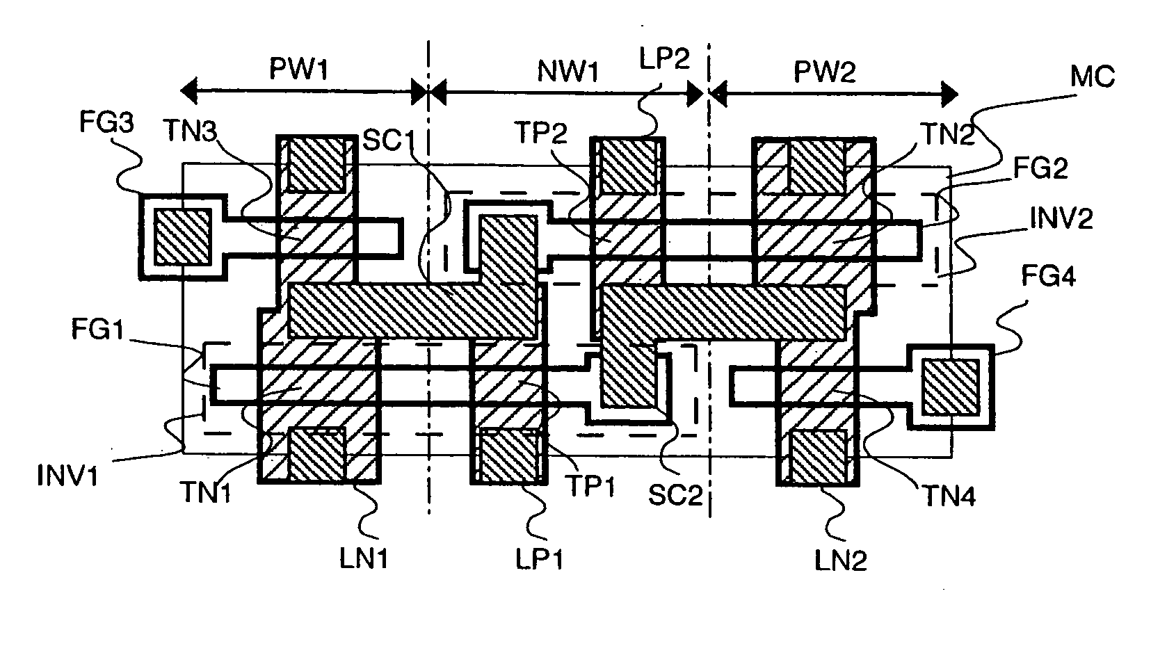
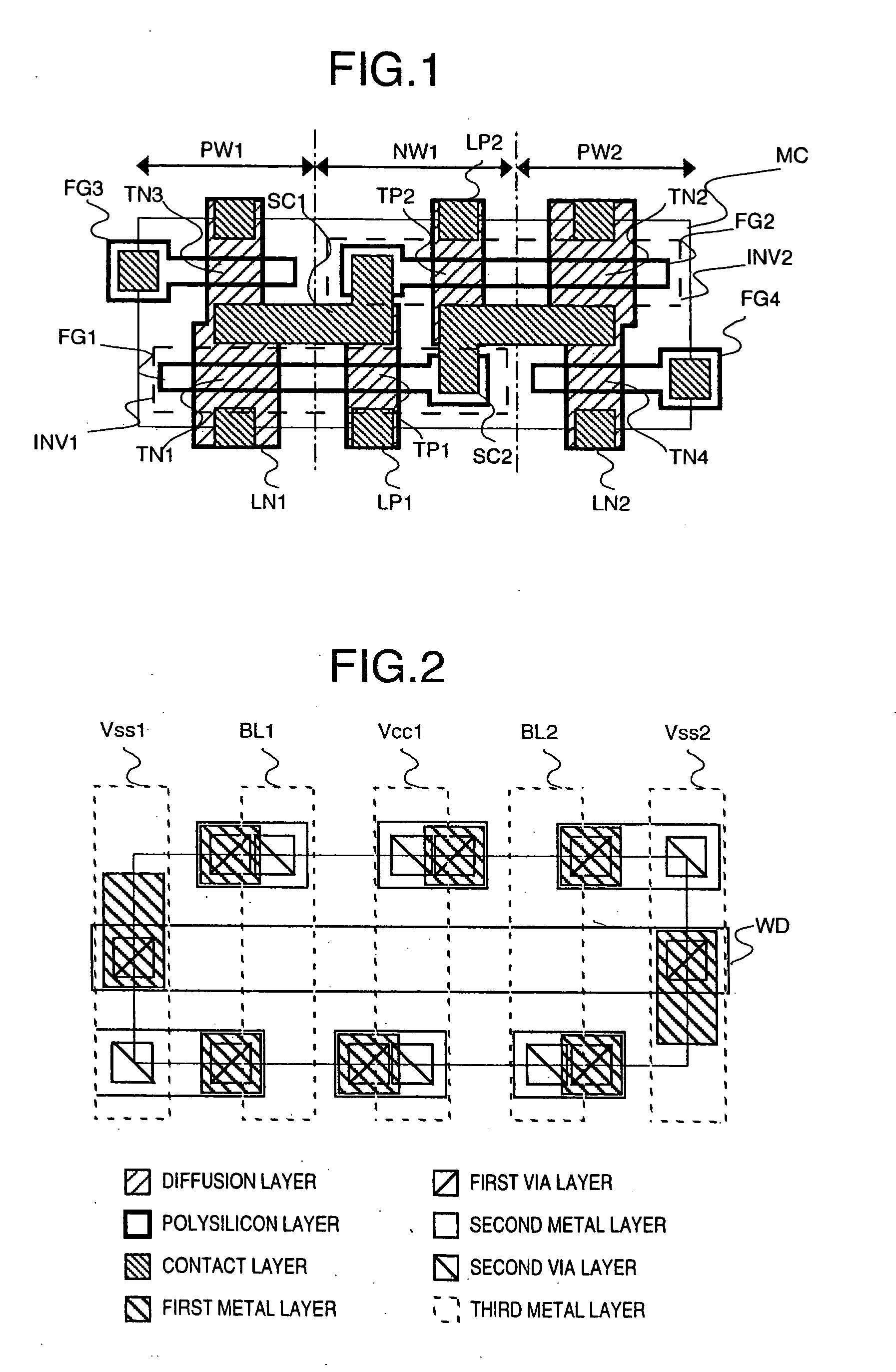
[0039] Referring to FIGS. 1 and 2, SRAM cell layout MC embodying the invention. FIG. 1 illustrates-well regions and diffusion layers plus a polycrystalline silicon interconnect lead layer, as well as contacts, all of which are formed in or over a semiconductor substrate FIG. 2 depicts a first layer serving as a metal lead layer, via holes 1, a second layer serving as a metal lead layer, via holes 2, and a third layer serving as a metal lead layer. Symbols used in FIGS. 1 and 2 are indicated at the lower part of FIG. 2.

[0040] An N-channel type MOS transistor TN1 formed in a P-type semiconductive well region PW1 and a P-channel type MOS transistor-TP1 formed in an N-type well region NW1 constitute an inverter INV1. In addition, an N-channel MOS transistor TN2 formed in P-type well region PW2 and a P-channel MOS transistor TP2 formed in N-type well region NW1 constitute an inverter INV2.

[0041] An output node of the inverter INVL is electrically connected by a contact SC1 to an input ...

embodiment 2

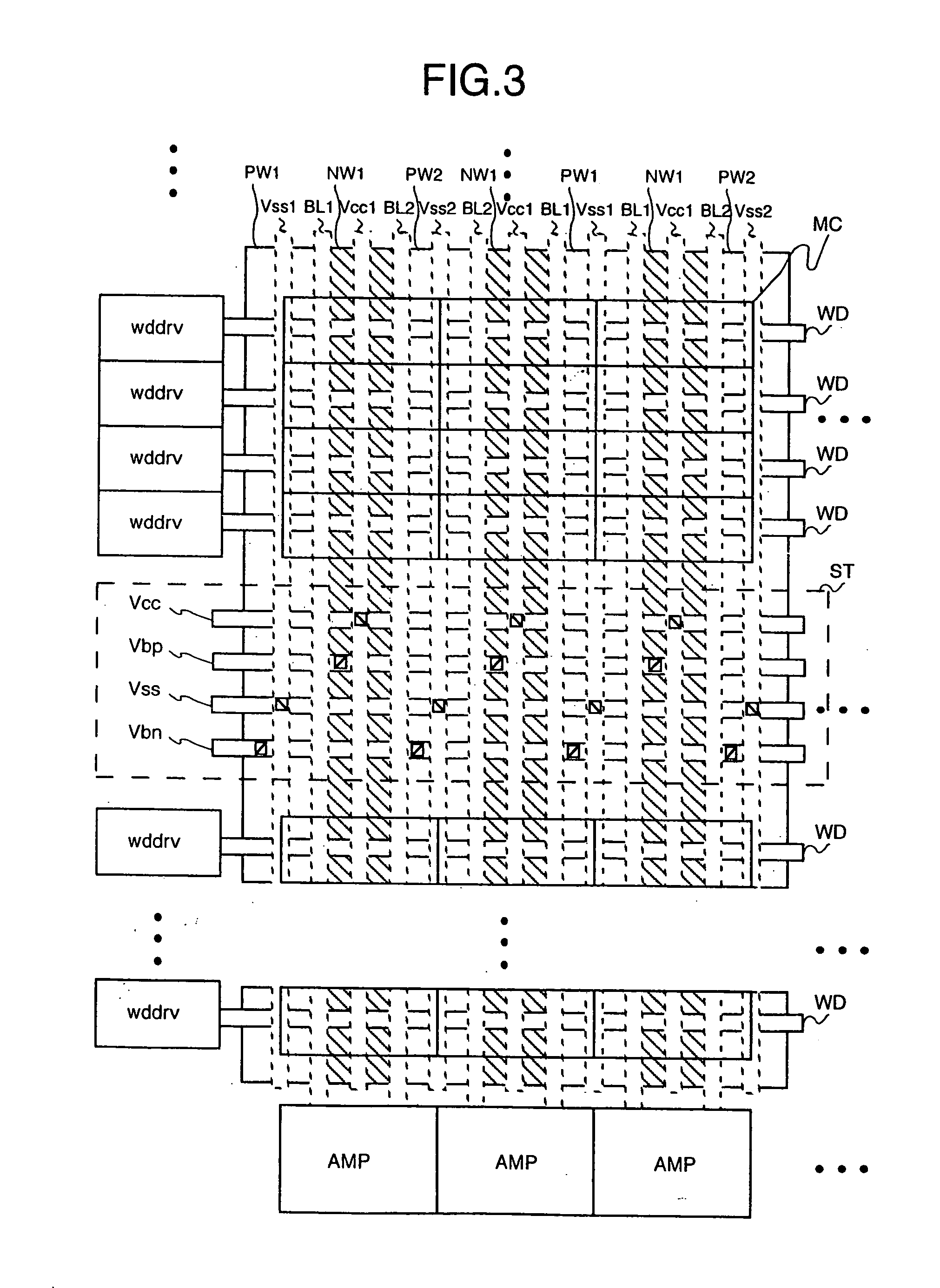
[0049] Turning to FIG. 3, an exemplary case is shown where the memory cells MC of Embodiment 1 are laid out into the form of an array. Symbols used herein are the same as those indicated at the lower part of FIG. 2.

[0050] The memory cells MC are organized into an array of 256 rows and 128 columns, by way of example. In view of the fact that these memory cells in Embodiment 1 are shorter in length in the longitudinal direction of the bit lines, the total length of the 256 rows of memory cells along the bit lines is shorter than that of prior art devices, thus increasing resultant operation speeds. Neighboring memory cells MC are disposed in linear symmetry with respect to a “y” axis whereas upper and lower adjacent memory cells MC are in linear symmetry with an “x” axis. In addition, specified regions ST for use in supplying more than one power supply voltage to the substrate are formed at the intermediate part of the array in such a manner that the regions ST extend parallel to wor...

embodiment 3

[0055]FIGS. 4 and 5 show a SRAM cell layout MC2 in accordance with Embodiment 3. Symbols as used in FIGS. 4-5 are the same as those in FIG. 2. Memory cell MC2 of Embodiment 3 is similar to the memory cell MC of Embodiment 1, with the exception that, as compared to Embodiment 1, in which the diffusion layer (LN1, LN2) is formed into a “T”-like planar shape, which resembles a Japanese battledore plate called “hagoita,” the diffusion layer (LN3, LN4) of Embodiment 4 is of a rectangular shape, and the contacts (SC1, SC2) are replaced with contacts (SC3, SC4) in the first layer serving as metal lead layers (M11, M12).

[0056] To attain stability, memory cells are typically designed so that the gate width of the N-channel MOS transistors (TN1, TN2) is one and a half times greater than that of the N-channel MOS transistors (TN3, TN4) However, in this case, the shape of the diffusion layers resembles a T-like planar shape, as shown in Embodiment 1, which in turn requires extra techniques, in...


PUM


Abstract

Prior known static random access memory (SRAM) cells are required that a diffusion layer be bent into a key-like shape in order to make electrical contact with a substrate with a P-type well region formed therein, which would result in a decrease in asymmetry leading to occurrence of a problem as to the difficulty in micropatterning. To avoid this problem, the P-type well region in which an inverter making up an SRAM cell is formed is subdivided into two portions, which are disposed on the opposite sides of an N-type well region NW1 and are formed so that a diffusion layer forming a transistor has no curvature while causing the layout direction to run in a direction parallel to well boundary lines and bit lines. At intermediate locations of an array, regions for use in supplying power to the substrate are formed in parallel to word lines in such a manner that one regions is provided per group of thirty two memory cell rows or sixty four cell rows.

Description

[0001] This application is a Continuation of application Ser. No. 11 / 042,172, filed Jan. 26, 2005 which is a Continuation of application Ser. No. 10 / 606,954, filed Jun. 27, 2003 (now abandoned), which is a Continuation of application Ser. No. 09 / 565,535, filed May 5, 2000 (now U.S. Pat. No. 6,677,649), the entire disclosures of which are hereby incorporated by reference.BACKGROUND OF THE INVENTION [0002] The present invention relates generally to semiconductor integrated circuit devices and, more particularly, to layout schemes of static random access memory (SPAN) cells. The invention also relates to semiconductor memory devices using such cells. [0003] One-port SRAM cells with complementary metal oxide semiconductor (CMOS) configurations are typically designed so that each cell consists essentially of six separate transistors. An exemplary layout of such cells has been disclosed, for example, in JP-A-10-178110 (laid open on Jun. 30, 1998). [0004] In the previously known SRAM cell ...

Claims


Application Information

Patent Timeline
Patent Type & Authority Applications(United States)
IPC IPC(8): G11C7/00H01L21/8244H01L27/11H01L27/10
CPCY10S257/904G11C11/412H10B10/00H10B10/12G11C11/417H01L29/4916H01L29/783
Inventor OSADA, KENICHIMINAMI, MASATAKAIKEDA, SHUJIISHIBASHI, KOICHIRO
Owner OSADA KENICHI
Learn More