Method for manufacturing power diode and equipment for the same

a technology of power diodes and manufacturing methods, applied in the direction of basic electric elements, electrical equipment, semiconductor devices, etc., can solve the problems of high complexity, inability to meet the requirements of production, so as to improve the concentration distribution of etching gas, simplify the etching process and the structure, and prevent the effect of unnecessary gas flow directions

Inactive Publication Date: 2006-03-09
ACTRON TECH
View PDF2 Cites 1 Cited by
  • Summary
  • Abstract
  • Description
  • Claims
  • Application Information

AI Technical Summary

Benefits of technology

[0010] Another objective of the present invention is to provide a method and equipment for manufacturing a power diode that use a shield plate to improve the concentration distribution of the etching gas inside the reaction vessel, prevent the unnecessary flow directions of the gas.
[0011] Still another objective of the present invention is to provide a method and equipment that can simplify the etching process and architecture for manufacturing a power diode. Thereby, the cost can be lowered and the quality of the products can be improved.

Problems solved by technology

However, using this method will cause different etching results for semiconductors with different impurity concentrations.
In addition, since the liquid etching method includes many necessary processing steps, its complexity is very high.
In the conventional manufacture method of power diode, since a lot of factors and steps must be considered and performed, the products usually have defects caused by improper handling.
Accordingly, as discussed above, the prior art still has some drawbacks that could be improved.

Method used


Image

  • Method for manufacturing power diode and equipment for the same
  • Method for manufacturing power diode and equipment for the same
  • Method for manufacturing power diode and equipment for the same

Examples


Embodiment Construction

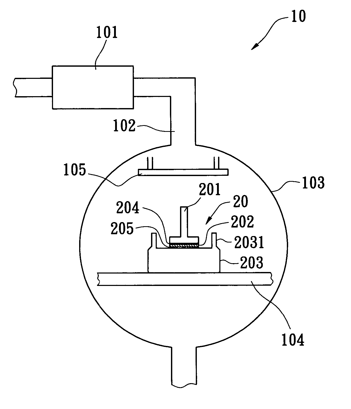
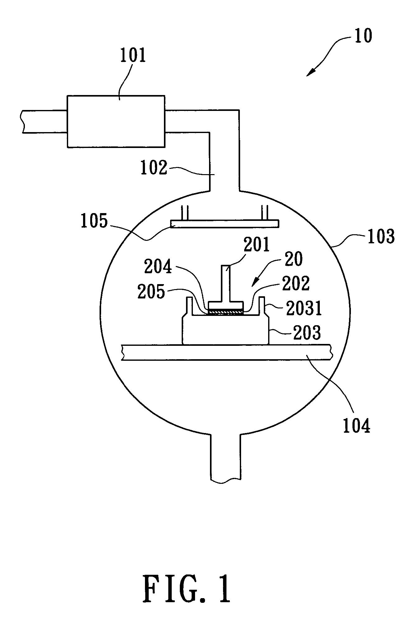
[0017] Reference is made to FIG. 1. The present invention provides a unit manufacturing equipment 10 to produce a power diode. Manufacturing equipment 10 includes a plasma generator 101, a pipe 102, a reaction vessel 103, a carrier 104 and a shield plate 105. The shield plate 105 is disposed directly under the outlet of the pipe 102 to control the flow direction of the input gas. The carrier 104 is used to carry a power diode 20. The manufacturing equipment 10 can perform a removal process on the power diode 20, i.e., the method of the present invention.

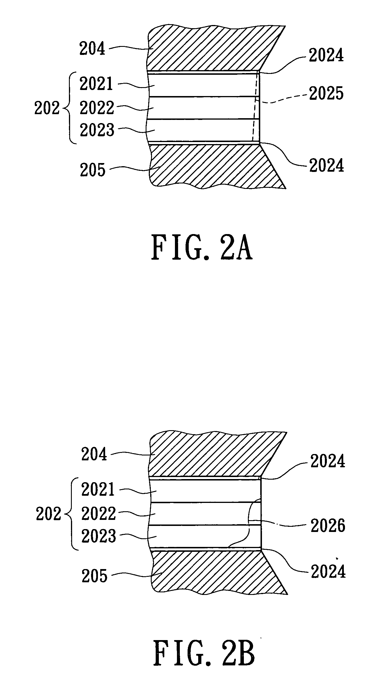
[0018] The power diode 20 has three main parts, including a top wire 201, a diode chip 202, and a cold base 203. Solder layers 204, 205 are used to integrate these three parts together. In addition, the cold base 203 has a protection plate 2031 surrounding the diode chip 202.

[0019] In the beginning of method according to the present invention, the manufacturing equipment 10 will provide a fluoride gas to the plasma generator 101. T...


PUM


Abstract

A method and equipment for manufacturing a power diode are described. More particularly, a manufacturing method and a unit of equipment used to remove an exposed portion of a P-N junction of a semiconductor (especially for power diodes) are described. The equipment has a reaction vessel having an input outlet and defining an airtight space inside. The power diode is placed inside the reaction vessel. A plasma generator is used to ionize an etching gas to produce free radicals and ions. The plasma generator is connected with the input outlet to flush the ionized etching gas into the reaction vessel. A shield plate is disposed under the input outlet of the reaction vessel to form a flow direction and a concentration distribution of the etching gas to etch a laterally exposed portion of the P-N junction.

Description

BACKGROUND OF THE INVENTION [0001] 1. Field of the Invention [0002] The present invention is directed to a method and equipment for manufacturing a power diode, and more particularly, to a manufacturing method and equipment used to remove an exposed portion of a P-N junction of a semiconductor (especially for power diode). [0003] 2. Description of Related Art [0004] In general, a conventional power diode has three parts, including a cold base, a diode chip and a top wire. These three parts will be soldered together. After soldering process, it is necessary to remove the laterally exposed portion of the P-N junction of the semiconductor to increase the blocking ability of the P-N junction. [0005] In the conventional manufacture method, the laterally exposed portion of the P-N junction is usually removed by using an alkaline solution, such as KOH solution, to perform an etching process. However, using this method will cause different etching results for semiconductors with different i...

Claims


Application Information

Patent Timeline
Patent Type & Authority Applications(United States)
IPC IPC(8): H01L21/332H01L21/302H01L21/8234
CPCH01L29/6609
Inventor SHEEN, CHARNG-GENG
Owner ACTRON TECH
Why Eureka
Try Eureka