Method of creating defect free high Ge content (>25%) SiGe-on-insulator (SGOI) substrates using wafer bonding techniques

a technology of sigeon-on-insulator and wafer bonding, which is applied in the direction of basic electric elements, electrical equipment, semiconductor devices, etc., can solve the problems of void generation problems, severe blistering, and bubbling of bonded sgoi with its high ge content layer, and achieves low defect densities, reduces or eliminates any bonding induced defects, and increases the bonding yield of sgoi substrates

Active Publication Date: 2006-03-16
GLOBALFOUNDRIES US INC
View PDF4 Cites 37 Cited by
  • Summary
  • Abstract
  • Description
  • Claims
  • Application Information

AI Technical Summary

Benefits of technology

[0009] The present invention describes a method for achieving a substantially defect free SGOI substrate which includes a SiGe layer that has a high Ge content of greater than about 25 atomic % using a low temperature wafer bonding technique. The term “substantially defect free” is used in the present application to denote a SiGe layer that has a defect density, including misfits, threading defects, microtwins, stacking faults and other defects, that is about 104 to about 105 defects / cm2 or less, and is dictated by the initial SiGe buffer. Currently, high temperature RT-CVD growth techniques are being developed to grow high content SiGe buffers with low defect densities in the range of 103-104 defects / cm2. The wafer bonding process described in the present application includes an initial prebonding annealing step that is capable of forming a bonding interface comprising elements of Si, Ge and O, i.e., an interfacial SiGeO layer, between the SiGe layer and an oxide, which substantially eliminates or reduces any bonding induced defects and increases the bonding yield of the SGOI substrates.
[0010] Specifically, by subjecting an initial high Ge content SiGe wafer covered with a layer of deposited low temperature oxide (later serving as the buried oxide, BOX) to an appropriate thermal annealing step, a bonding interface comprising a thin layer of SiGeO or a mixture of Si / Ge oxide is formed in the present invention between the SiGe layer and the low temperature oxide. This interdiffused or oxygen-enriched SiGeO layer, i.e., the bonding interface or interfacial SiGeO layer, is believed to act as a gettering layer to either trap defects or prevent volatile gases or residuals (such as hydroxyl group, hydrogen, oxygen, and the like) from penetrating into the SiGe film from either the BOX layer or the bonded BOX / SiGe interface during a densificaton step and can thereby reduce or eliminate any undesirable blistering due to entrapped, residual volatile species.
[0011] In addition, the bonding interface layer, i.e., the interfacial SiGeO layer, can further serve to suppress hydrogen from diffusing or migrating from the high concentration region (of the smart cut region) to the SiGe / BOX interface during the subsequent post-bonding anneal and wafer splitting anneal steps. If no such anneal step is implemented and no such interfacial layer exists, the bonded SGOI with its high Ge content layer will suffer from severe blistering, bubbling, and void generation problems typically associated with a low yield in wafer bonding process. Nevertheless, the thickness of the interfacial SiGeO layer can be tailored by adjusting the anneal temperature and time.

Problems solved by technology

If no such anneal step is implemented and no such interfacial layer exists, the bonded SGOI with its high Ge content layer will suffer from severe blistering, bubbling, and void generation problems typically associated with a low yield in wafer bonding process.

Method used


Image

  • Method of creating defect free high Ge content (>25%) SiGe-on-insulator (SGOI) substrates using wafer bonding techniques
  • Method of creating defect free high Ge content (>25%) SiGe-on-insulator (SGOI) substrates using wafer bonding techniques
  • Method of creating defect free high Ge content (>25%) SiGe-on-insulator (SGOI) substrates using wafer bonding techniques

Examples


example

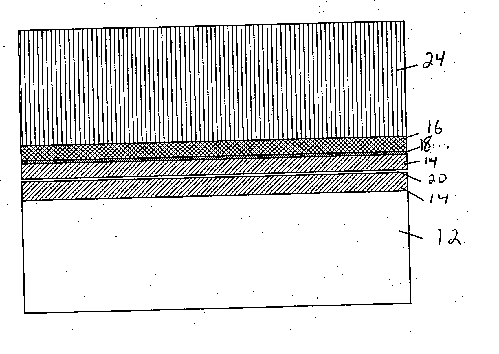
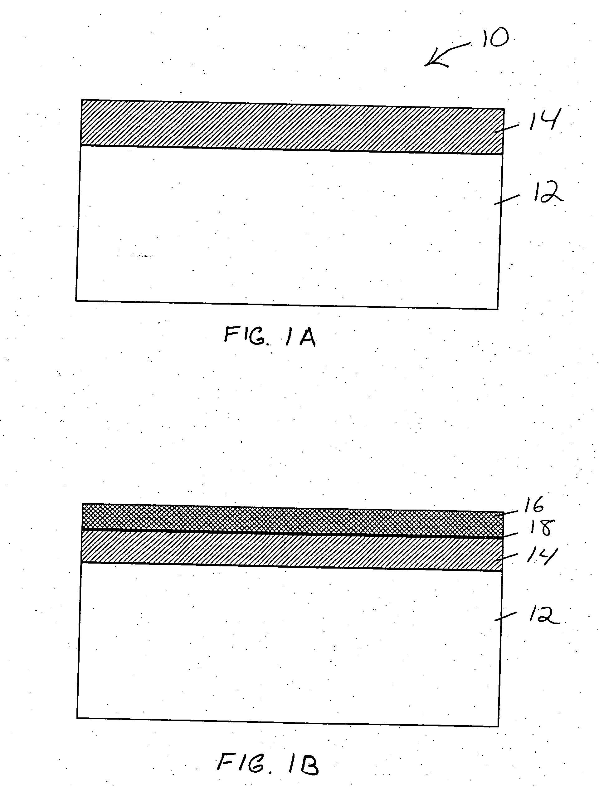
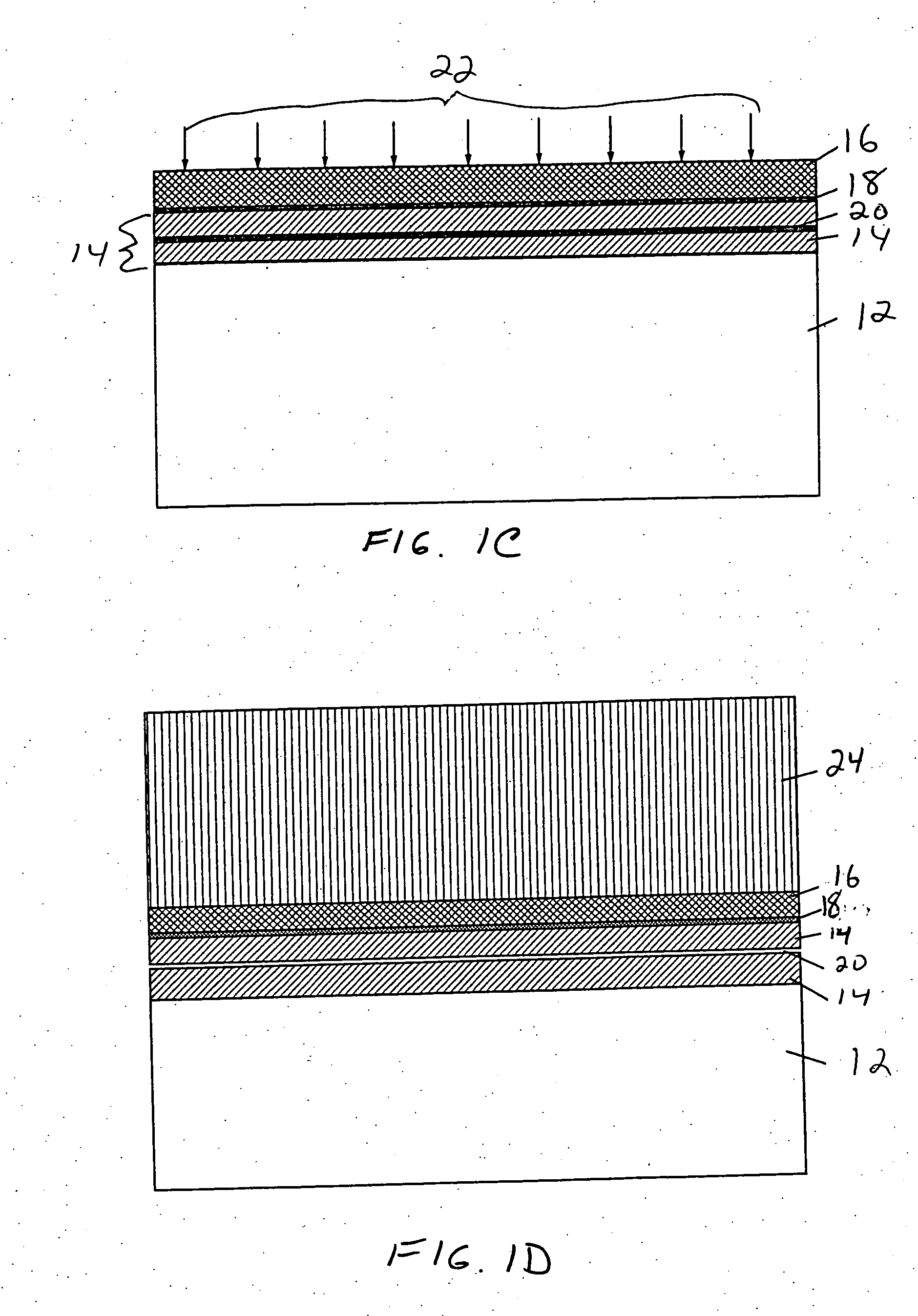
[0060] In this example, a substantially low defect, high Ge content SGOI wafer is provided utilizing the processing steps of the present invention. This process follows the general procedure outlined above, but provides a more detailed and specific implementation of the inventive method. The process starts with a bulk Si wafer that was cleaned by conventional RCA wet cleans. A graded SiGe buffer layer was then deposited on the bulk Si wafer utilizing a conventional deposition process. The total thickness of the SiGe buffer layer was about 1.5 to 2.0 μm. Chemical mechanical polishing (CMP) with a down-force of about 1.5 psi was used to smooth the surface of the SiGe buffer layer and simultaneously to reduce the thickness of the buffer layer by an amount of a couple of hundred nanometers. Afterwards, and in addition to the conventional brush cleaning normally associated with CMP, the wafer was further cleaned in a modified RCA solution several times to remove the particles and the res...


PUM

PropertyMeasurementUnit
thicknessaaaaaaaaaa
thicknessaaaaaaaaaa
temperatureaaaaaaaaaa

Abstract

A method for achieving a substantially defect free SGOI substrate which includes a SiGe layer that has a high Ge content of greater than about 25 atomic % using a low temperature wafer bonding technique is described. The wafer bonding process described in the present application includes an initial prebonding annealing step that is capable of forming a bonding interface comprising elements of Si, Ge and O, i.e., interfacial SiGeO layer, between a SiGe layer and a low temperature oxide layer. The present invention also provides the SGOI substrate and structure that contains the same.

Description

[0001] The present invention described herein was made with U.S. Government support under Contract No. N66001-00-C-8086 awarded by The Department of the Navy. The U.S. Government thus has certain rights in this invention.FIELD OF THE INVENTION [0002] The present invention relates to the fabrication of a SiGe-on-insulator (SGOI) substrate, and more particularly, to a substantially defect free, high Ge content (>25 atomic %) SGOI substrate as well as method of fabricating the same. The method of the present invention includes a wafer bonding technique that is capable of forming an interfacial bonding layer that includes elements of Si, Ge and O. The interfacial bonding layer is referred to herein as an interfacial SiGeO layer. BACKGROUND OF THE INVENTION [0003] It is well known to those skilled in the art that strained silicon can enhance carrier mobility for both electrons and holes in comparison with bulk silicon. In addition, the degree of mobility enhancement strongly depends o...

Claims


Application Information

Patent Timeline
Patent Type & Authority Applications(United States)
IPC IPC(8): H01L29/12H01L21/18
CPCH01L21/0245H01L29/1054H01L21/76254H01L21/0251H01L21/20
Inventor CHU, JACK O.COBB, MICHAEL A.SAUNDERS, PHILIP A.SHI, LEATHEN
Owner GLOBALFOUNDRIES US INC
Why Eureka
Try Eureka