Quantum nano-composite semiconductor laser and quantum nano-composite array

a semiconductor laser and quantum nano-composite technology, applied in semiconductor laser arrangements, semiconductoronductors, nanoinformatics, etc., can solve the problems of increasing the cost of production, limiting the diffusion of products in the industry, and adding the leak path of the drive curren

Inactive Publication Date: 2006-03-16
NAT INST OF ADVANCED IND SCI & TECH +1
View PDF8 Cites 17 Cited by
  • Summary
  • Abstract
  • Description
  • Claims
  • Application Information

AI Technical Summary

Benefits of technology

[0022] For the purpose of accomplishing the object mentioned above, the first aspect of this invention is directed toward providing a quantum nano-structure semiconductor laser comprising a grooved semiconductor substrate furnished with a plurality of V-grooves individually extended in directions perpendicular to a direction of a laser beam and mutually disposed in parallel along the direction of the laser beam and a plurality of quantum wires formed one on each of the V-grooves by selective growth of a Group III-V compound, the plurality of quantum wires being mutually disposed in parallel along the direction of advance of the laser beam with a period of an integer times of a quarter wavelength in a medium of a laser active layer and disposed individually as an active layer region of a limited length corresponding to a width of stripes of laser. Thus, this invention is capable of providing a quantum nano-structure semiconductor laser that satisfies at least one, or preferably both, of the reduction of the threshold and the stabilization of the frequency of oscillation more satisfactorily than the conventional countertype.

Problems solved by technology

Such multiple cycles of lithography and crystal growth results in boosting the cost of production and impeding the dissemination of the product in industry.
Further, since the re-growth interface exists in the neighborhood of the active layer, it causes an additional leak path of the drive current and increases the threshold current.
The technique of this nature, therefore, has its limits in terms of principle and cannot continue to be similarly useful in the future.
In the case of submicron gratings having the shortest possible period relative to the distance of diffusion of Ga atoms adhering to the surface of the substrate, however, it is generally considered difficult to attain the necessary growth while a specific profile of crystal growth is retained.
In fact, the growth was impossible at first.
According to the technique prevalent at the time of disclosure of this publication, however, the profile of V-grooves was seriously impaired when the height of superposed layers reached a level exceeding 1 μm.

Method used


Image

  • Quantum nano-composite semiconductor laser and quantum nano-composite array
  • Quantum nano-composite semiconductor laser and quantum nano-composite array
  • Quantum nano-composite semiconductor laser and quantum nano-composite array

Examples


Embodiment Construction

[0045] This invention will be described more specifically below with reference to the drawing annexed hereto.

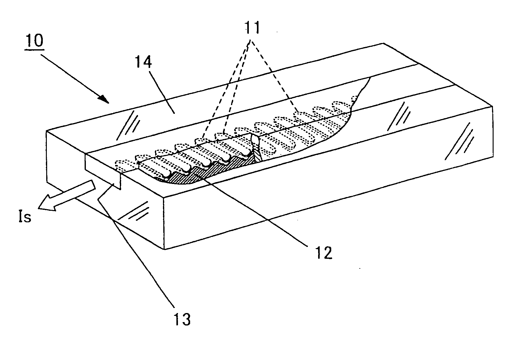
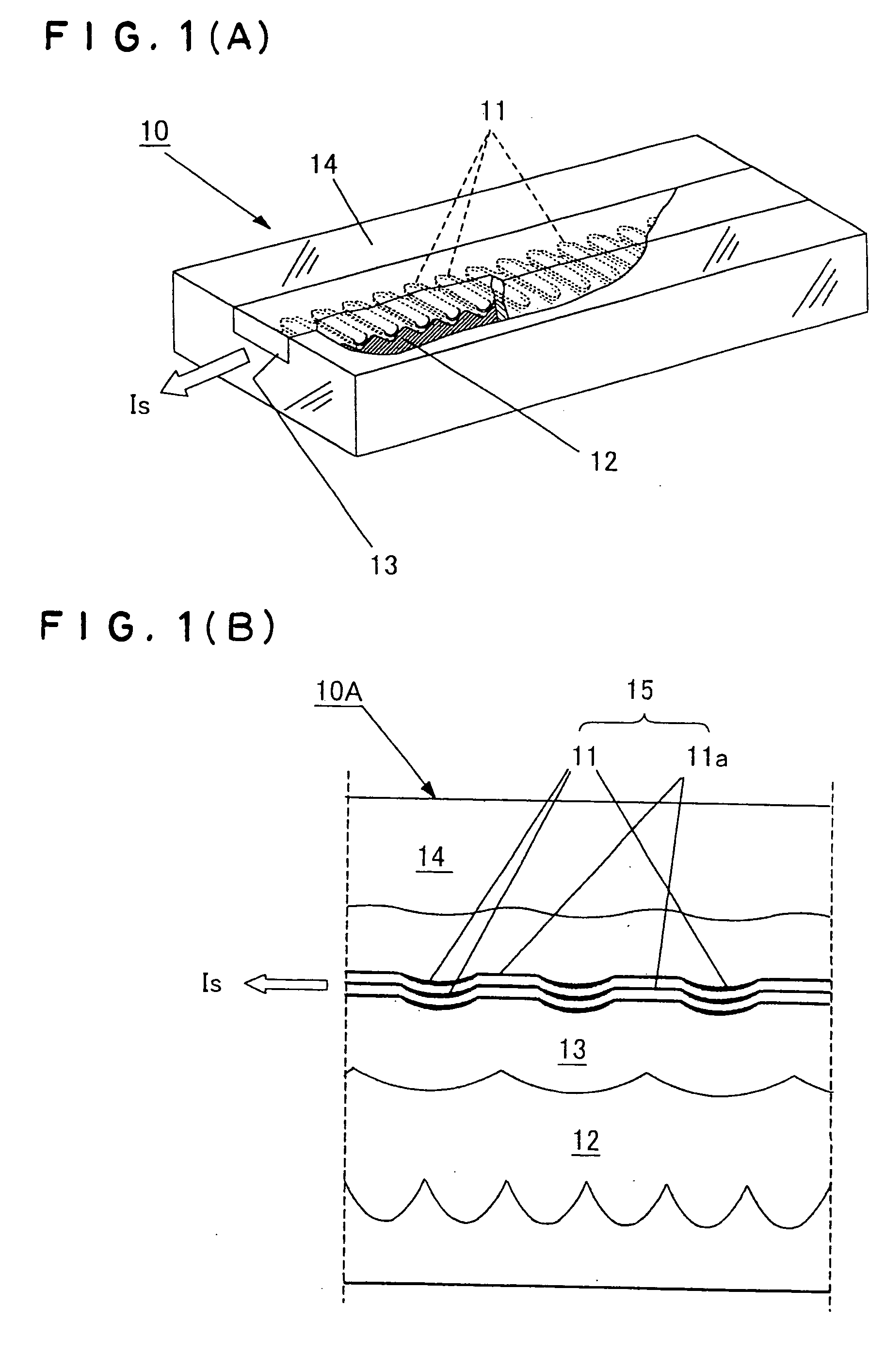
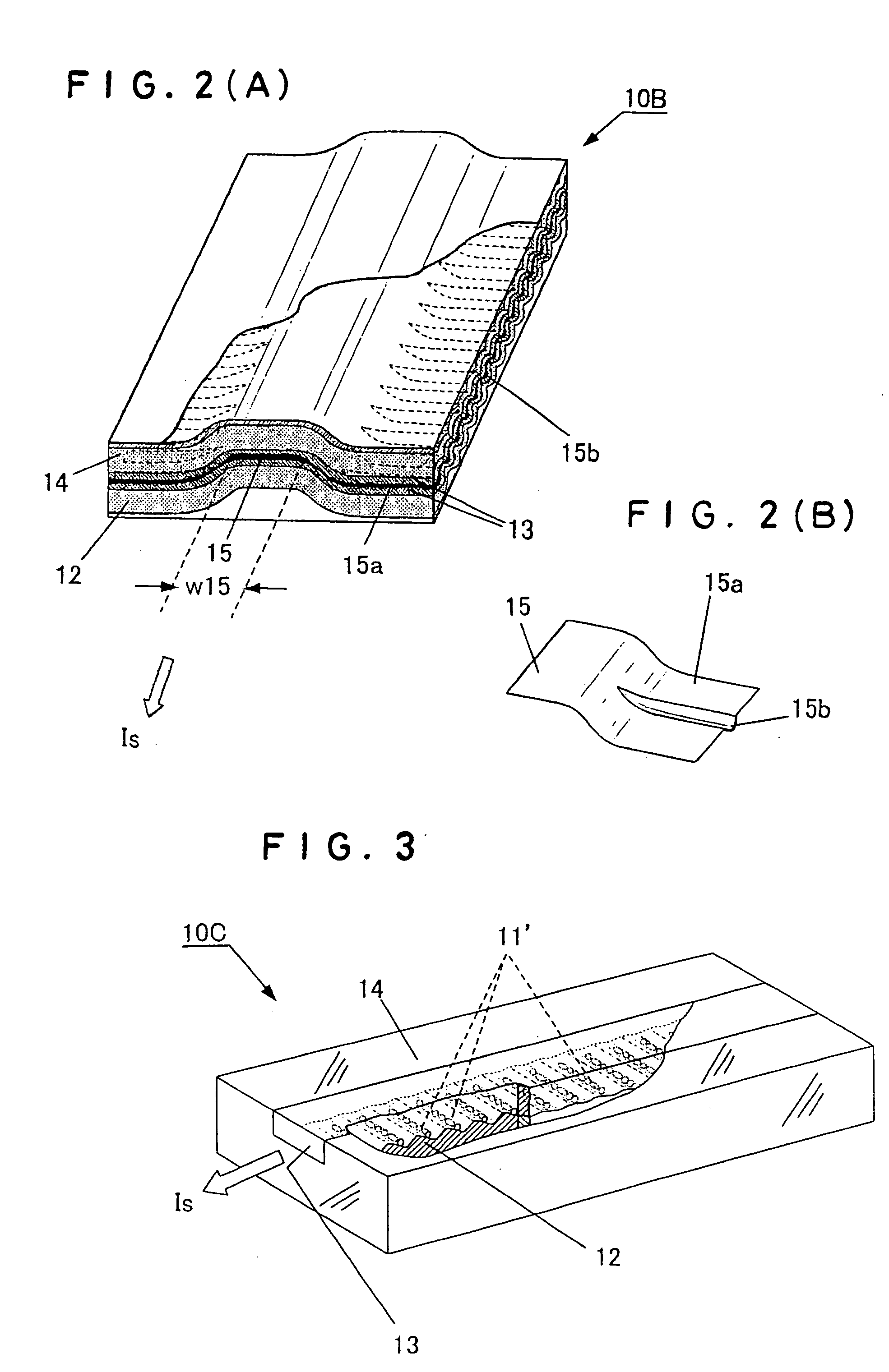
[0046] In FIG. 1, one example of the structure of a distributed feedback semiconductor laser 10 as one preferred embodiment of a quantum nano-structure semiconductor laser constructed in accordance with this invention. Basically, the whole structure is manufactured by the method of production disclosed in Japan Patent Application No. 2000-404645 (JP-A 2002-204033). It is provided with an active layer which, as viewed in the direction of light emission Is, comprises a V-groove substrate having a plurality of V-grooves disposed in parallel thereon and limited-length GaAs or InGaAs quantum wires 11 individually formed in V-groove regions of the V-groove substrate and typically measuring 5 to 20 nm in thickness and 10 to 50 nm in the size in the direction of laser beam emission Is and 0.5 to 2 μm in the size (width) of the direction perpendicular to the direction of laser beam e...


PUM


Abstract

On a grooved semiconductor substrate having a plurality of V-grooves individually extended in directions perpendicular to a direction Is of advance of an oscillated laser beam and mutually disposed in parallel along the direction Is of advance of the laser beam, a plurality of quantum wires (11) are formed on the V-grooves by selective growth of a Group III-V compound. The plurality of quantum wires are adapted to serve as limited-length active layer regions mutually disposed in parallel along the direction Is of advance of the laser beam with a period of an integer times of a quarter wavelength in a medium of a laser active layer and individually corresponding to stripe widths of laser. Consequently, a quantum nano-structure semiconductor laser satisfying at least one, or preferably both, of the decrease of a threshold and the stabilization of an oscillation frequency as compared with a conventional countertype can be provided.

Description

TECHNICAL FIELD [0001] This invention relates to a quantum nano-structure semiconductor laser that is particularly effective for application to a distributed feedback (DFB) semiconductor laser and to improvements in and concerning a quantum nano-structure array applicable significantly to various optically functioning devices. BACKGROUND ART [0002] In the semiconductor lasers, the distributed feedback semiconductor laser that is provided in the direction of advance of a waveguide with periodic structures for refractivity and gain will discharge a very important role as a device for use in the future Wavelength Division Multiplexing (WDM) operation in respect that it is capable of controlling an oscillating wavelength exactly and it facilitates integration because it obviates the necessity of a step of cleavage indispensable as in the Fabry-Perot laser. [0003] The first problem that is encountered by the distributed feedback semiconductor laser pertains to simplification of the proce...

Claims


Application Information

Patent Timeline
Patent Type & Authority Applications(United States)
IPC IPC(8): H01S5/00H01L21/20H01L21/205H01L29/12H01S5/026H01S5/10H01S5/12H01S5/22H01S5/34H01S5/40
CPCB82Y10/00H01L21/02636H01L29/127H01S5/0265H01S5/1053H01S5/1206H01S5/1228H01S5/1237H01S5/22H01S5/341H01S5/3412H01S5/4031H01L21/02392H01L21/02395H01L21/0243H01L21/02433H01L21/02546H01L21/0259B82Y20/00H01S5/34H01S5/40
Inventor OGURA, MUTSUO
Owner NAT INST OF ADVANCED IND SCI & TECH
Why Eureka
Try Eureka