Jitter self test

a jitter and self-testing technology, applied in the direction of transmission monitoring, line-transmission details, pulse techniques, etc., can solve the problems of jitter errors in data being transmitted, possible degradation of system performance, and expensive high-speed equipment to measure jitter, and achieve time-consuming and time-consuming use. , the effect of improving the accuracy of measuremen

Inactive Publication Date: 2006-03-16
SILICON LAB INC
View PDF9 Cites 55 Cited by
  • Summary
  • Abstract
  • Description
  • Claims
  • Application Information

AI Technical Summary

Problems solved by technology

Those high speed clocks typically include some level of jitter, which can lead to bit errors in the data being transmitted and possible degradation of system performance.
Jitter may be caused by noise introduced into the system from any of a variety of sources.
For high speed integrated circuits, measuring jitter can require expensive high speed equipment that can be time consuming to use.
In addition, the external equipment allows noise sources to be coupled into the integrated circuit during measurement that may adversely affect the jitter measurement.

Method used


Image

  • Jitter self test
  • Jitter self test
  • Jitter self test

Examples


Embodiment Construction

)

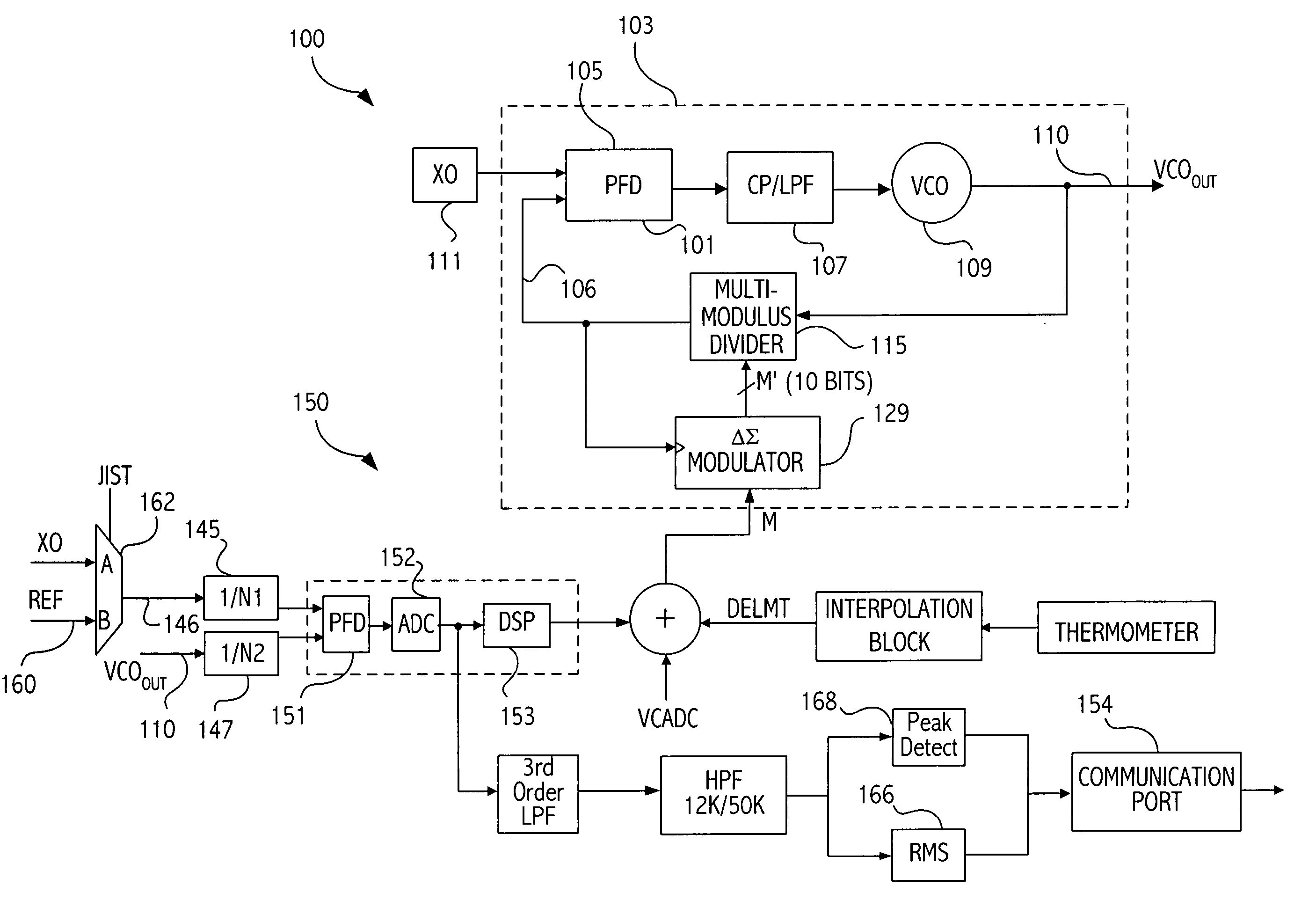
[0015] Referring to FIG. 1, illustrated is an exemplary embodiment of a dual loop architecture 100 that can advantageously exploit jitter self test concepts described herein. The dual loop architecture includes a digitally controlled oscillator (DCO) 103 also referred to herein as the “inner loop.” The digitally controlled oscillator 103 is formed as a phase-locked loop and includes a phase / frequency detector (PFD) 105, a charge pump / loop filter 107 and a voltage controlled oscillator 109. The crystal (or surface acoustic wave (SAW) device) 111 supplies a timing reference to the DCO 103 as one input to the phase and frequency detector 105. Phase and frequency detector 105 generates an error term of the difference between the crystal oscillator input and the feedback from the VCO 109. Note that the feedback is supplied by multi-modulus divider block 115. In certain applications, the divider value of the “inner loop”103 is controlled by an “outer loop”150. An exemplary outer loop inc...


PUM


Abstract

Jitter is measured by receiving a first reference signal at a first phase-locked loop (PLL) circuit and generating at an output of the first phase-locked loop circuit an output signal based at least in part on the first reference signal, the output signal including a jitter component to be measured. A signal corresponding to the output signal and a signal corresponding to the first reference signal are compared in a phase detector of a second phase-locked loop circuit. A value corresponding to an output of the comparison is stored that includes information indicative of the measured jitter component.

Description

CROSS-REFERENCE TO RELATED APPLICATION(S) [0001] This application claims benefit under 35 U.S.C. § 119(e) of application Ser. No. 60 / 610,061, filed Sep. 15, 2004, entitled “Jitter Self Test”, naming Ligang Zhang as inventor.BACKGROUND [0002] 1. Field of the Invention [0003] This application relates to integrated circuit devices more particularly to testing for jitter present in integrated circuit devices. [0004] 2. Description of the Related Art [0005] Many applications, such as optical transmission systems, use high speed clocks to synchronize the flow of data. Those high speed clocks typically include some level of jitter, which can lead to bit errors in the data being transmitted and possible degradation of system performance. Jitter is the variation in clock output frequency or phase from a desired output frequency or phase and can occur for a number of reasons. Jitter may be caused by noise introduced into the system from any of a variety of sources. An important area of jitter...

Claims


Application Information

Patent Timeline
Patent Type & Authority Applications(United States)
IPC IPC(8): H03D3/24H03L7/06
CPCH03L7/087H03L7/0992H04L1/205H03L7/1976H03L7/197
Inventor ZHANG, LIGANG
Owner SILICON LAB INC
Why Eureka
Try Eureka