Strained finfet cmos device structures

a technology of finfet and device structure, applied in the field of finfet devices, can solve the problems of limited improvement of cmos circuits, and achieve the effects of enhancing device performance, enhancing mobility, and enhancing mobility

Inactive Publication Date: 2006-03-16
GLOBALFOUNDRIES US INC
View PDF89 Cites 192 Cited by
  • Summary
  • Abstract
  • Description
  • Claims
  • Application Information

AI Technical Summary

Benefits of technology

[0006] This invention is directed to a novel strained FinFET device structures for enhanced mobility. The integration scheme incorporates a new process flow that induces compressive stress in the longitudinal direction for the p-FinFET while also inducing tensile stress in the longitudinal direction for the n-FinFET. These stresses significantly enhance mobility and, thus, enhance device performance. In the invention described herein, the longitudinal stress induced in the channel is enhanced considerably from what can be obtained in standard planar MOSFETs, because the stressing film is applied from two sides of a thin FinFET, instead of on the surface of an SOI layer or bulk substrate.
[0007] It is a principal object of the present invention to enhance mobility in double gate CMOS device structures.
[0008] It is an additional object of the present invention to enhance mobility in FinFET device structures.
[0009] It is a further object of the present invention to improve methods of fabricating strained FinFET device structures.

Problems solved by technology

This prior art method is directed at improving nFET mobility and, therefor, only limited improvement in CMOS circuits can be attained.

Method used


Image

  • Strained finfet cmos device structures
  • Strained finfet cmos device structures
  • Strained finfet cmos device structures

Examples


Embodiment Construction

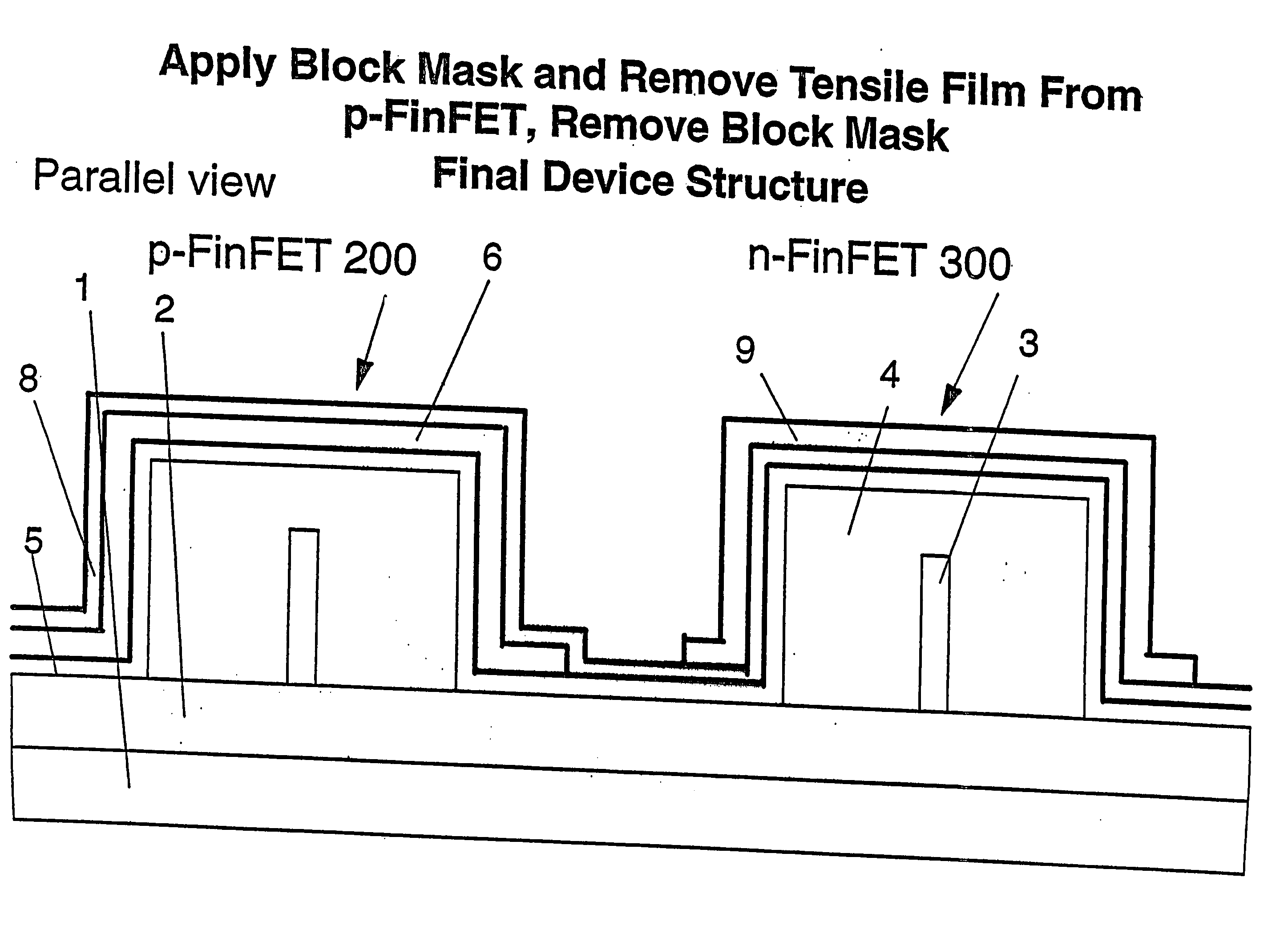
[0014] The present invention is directed to a novel FinFET semiconductor device structure and a method of manufacturing such structure. A preferred final structure according to the present invention is shown in FIGS. 16, 17.

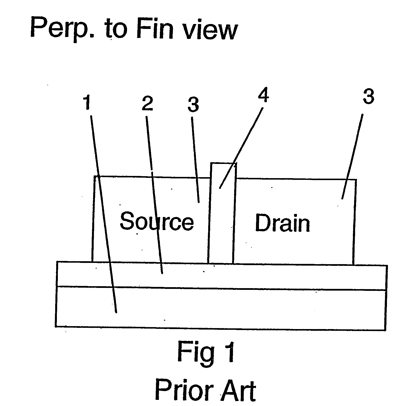
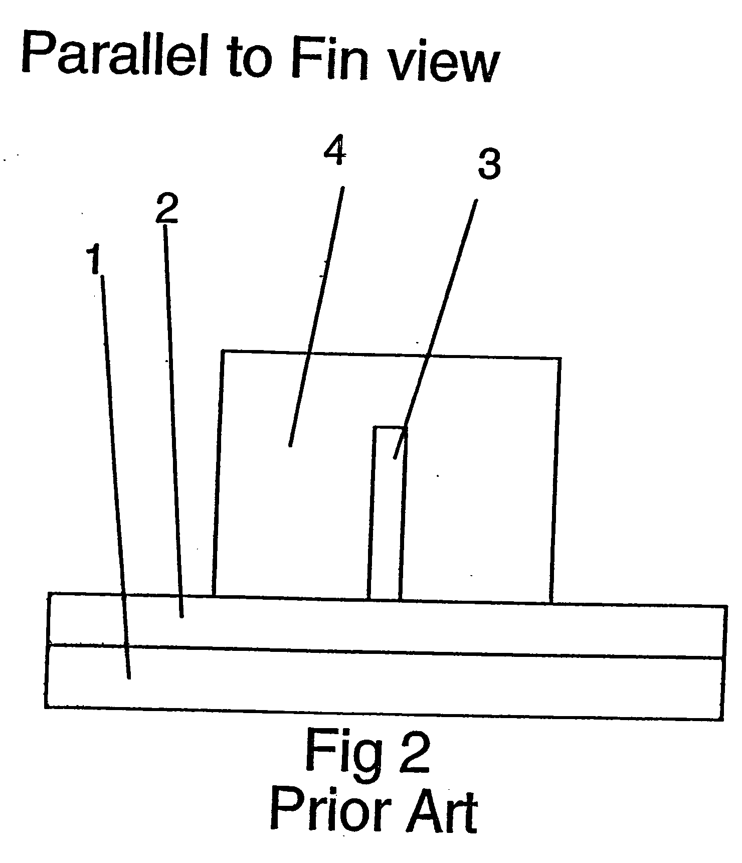
[0015] Referring now to the remaining figures and FIGS. 1-3 in particular, there are shown known FinFET devices (FIGS. 1, 2) and device structures (FIG. 3).

[0016] To begin, standard or conventional FinFET device manufacture processing is followed through the patterning and etching of the Fins, formation of gate dielectric and conductors, sidewall spacers (not shown), source / drain doping, and salicidation. Following salicidation, the gate sidewall spacers are removed, to facilitate the processing which will induce strain in the Fins according to the present invention.

[0017] More particularly, as described with reference to FIG. 3, an SOI wafer, for example, is provided. The SOI wafer includes a substrate 1, disposed underneath a buried SiO2 layer 2 as shown in ...


PUM


Abstract

A semiconductor device structure, includes a PMOS device 200 and an NMOS device 300 disposed on a substrate 1,2, the PMOS device including a compressive layer 6 stressing an active region of the PMOS device, the NMOS device including a tensile layer 9 stressing an active region of the NMOS device, wherein the compressive layer includes a first dielectric material, the tensile layer includes a second dielectric material, and the PMOS and NMOS devices are FinFET devices 200, 300.

Description

TECHNICAL FIELD [0001] The present invention relates to double gate semiconductor device structures and, more particularly, to FinFET devices. BACKGROUND ART [0002] Double gate semiconductor device structures are promising candidates for future generation microelectronics devices, because of the ability to obtain near ideal sub-threshold slope, absence of body-effect, immunity to short-channel effect, and very high current driveability. One double gate device structure of technological relevance is the FinFET. The FinFET is particularly attractive because of the relative simplicity of manufacture compared to other double gate devices. The channel for the FinFET is a thin rectangular island of Si, commonly referred to as the Fin. The gate wraps around the Fin so that the channel is gated on both sides of the vertical portions of the Fin structure, providing gate control which is superior to planar single gate MOSFETs. [0003] FinFETs are well known. See, for example, U.S. Pat. No. 6,4...

Claims


Application Information

Patent Timeline
Patent Type & Authority Applications(United States)
IPC IPC(8): H01L21/84H01L27/12
CPCH01L21/84H01L29/785H01L29/7843H01L27/1203
Inventor DORIS, BRUCEBCHIDAMBARRAO, DURESETILEONG, MEIKEIMANDELMAN, JACKA
Owner GLOBALFOUNDRIES US INC
Why Eureka
Try Eureka