Photosensitive bonding package structure

a technology of photosensitive packaging and packaging, applied in the field of chip package structure, can solve the problems of reducing the production cost of these photosensitive packages, and achieve the effect of reducing the horizontal width and the area of the packaged photosensitive devi

Inactive Publication Date: 2006-03-23
ADVANCED SEMICON ENG INC
View PDF21 Cites 16 Cited by
  • Summary
  • Abstract
  • Description
  • Claims
  • Application Information

AI Technical Summary

Benefits of technology

[0009] Accordingly, at least one objective of the present invention is to provide a photosensitive bonding package structure whose circuit substrate has an area almost equal the area occupied by the photosensitive region of a photosensitive device. Thus, the horizontal width and area of the packaged photosensitive device is reduced.

Problems solved by technology

Since the packaged photosensitive chip can integrate with other control circuits, analogue-to-digital (A / D) converters and digital processing signals, the production cost of these photosensitive packages has dropped considerably.

Method used


Image

  • Photosensitive bonding package structure
  • Photosensitive bonding package structure
  • Photosensitive bonding package structure

Examples


Embodiment Construction

[0021] Reference will now be made in detail to the present preferred embodiments of the invention, examples of which are illustrated in the accompanying drawings. Wherever possible, the same reference numbers are used in the drawings and the description to refer to the same or like parts.

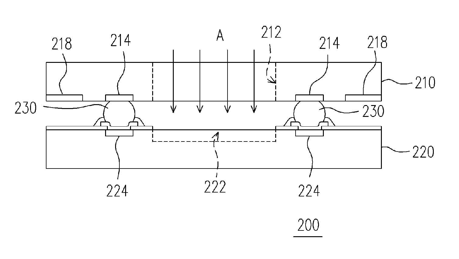
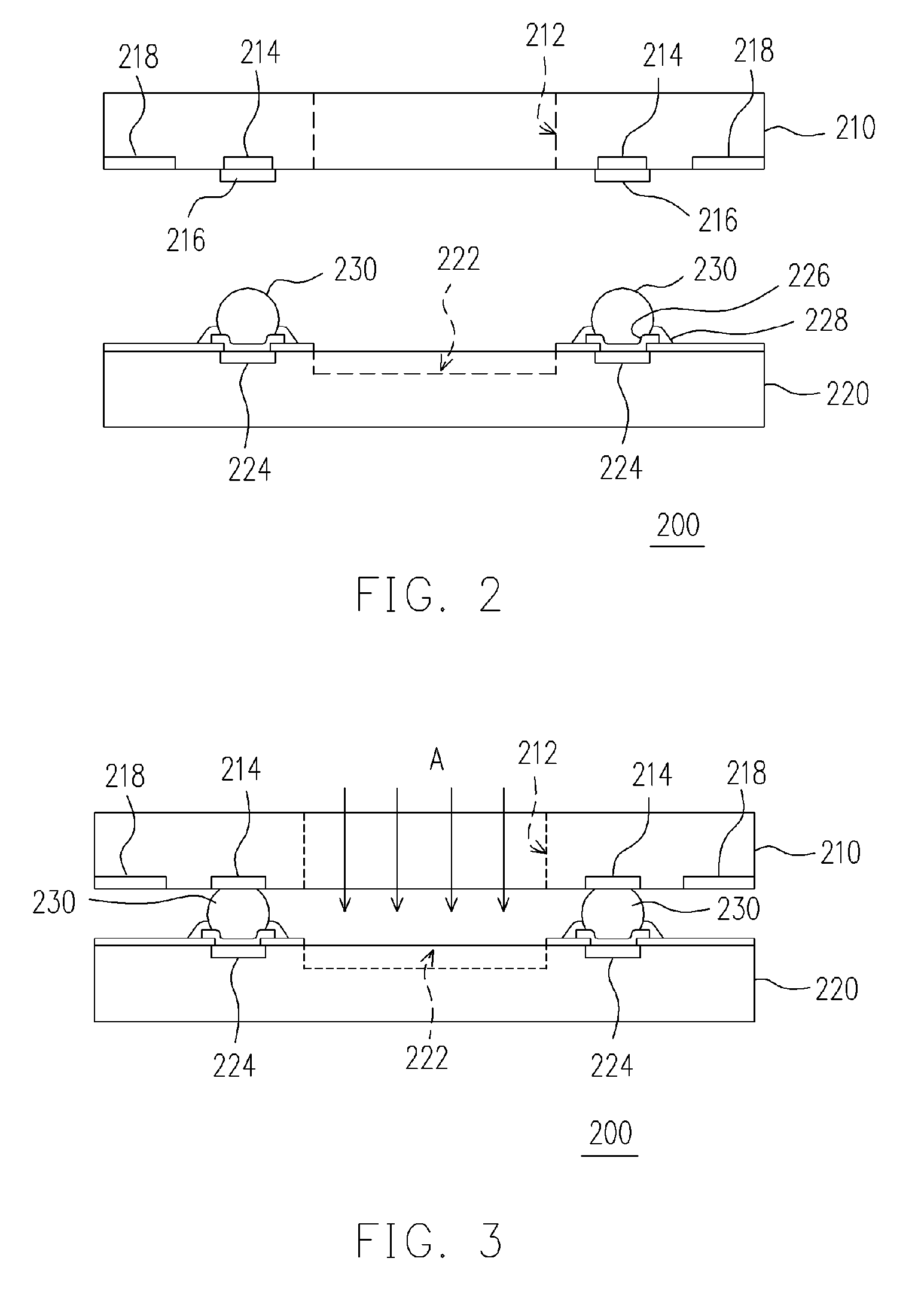
[0022]FIGS. 2 and 3 are schematic cross-sectional views showing a split-up and an assembled photosensitive bonding package according to one preferred embodiment of the present invention. As shown in FIG. 2, a circuit substrate 210 with a light incident area 212 is positioned above a photosensitive device 220. Thereafter, as shown in FIG. 3, the circuit substrate 210 is aligned with a plurality of bumps 230 on the photosensitive device 220 so that the two are electrically connected to form a photosensitive bonding package structure.

[0023] Before assembling the circuit substrate 210 and the photosensitive device 220 together, a light incident area 212 formed in the circuit substrate 210 is fabricate...


PUM


Abstract

A photosensitive bonding package structure mainly comprising a substrate, a photosensitive device and a plurality of bumps is provided. The substrate has a light incident area located near the central area of the substrate. The photosensitive device has a photosensitive area in a position corresponding to the light incident area so that the photosensitive device can receive a beam of incident light passing through the opening. In addition, the substrate has a plurality of inner contacts and corresponding outer contacts. Pads on the photosensitive device are connected to the inner contacts through bumps so that the electrical signals resulting from illuminating the photosensitive area is transmitted to the substrate.

Description

CROSS-REFERENCE TO RELATED APPLICATION [0001] This application claims the priority benefit of Taiwan application serial no. 93128512, filed on Sep. 21, 2005. All disclosure of the Taiwan application is incorporated herein by reference. BACKGROUND OF THE INVENTION [0002] 1. Field of the Invention [0003] The present invention relates to a chip package structure. More particularly, the present invention relates to a photosensitive bonding package structure. [0004] 2. Description of the Related Art [0005] With the rapid progress in electronic packaging techniques, a variety of semiconductor packages has been developed. It is now common to sent finished photosensitive chips (or wafers) to a wafer packaging facility for additional processing operations including wafer cutting, die attaching, curing, wire bonding, molding, ball implant and substrate loading. Finally, the finished products are quality inspected or functionally tested to ensure a good reliability. Since the packaged photosen...

Claims


Application Information

Patent Timeline
Patent Type & Authority Applications(United States)
IPC IPC(8): H01J40/14
CPCH01L27/14618H01L27/14632H01L27/14687H01L31/0203H01L2224/48227H01L2924/3025H01L2924/10253H01L2224/48091H01L2924/00014H01L2924/00
Inventor HUANG, TAI-YUAN
Owner ADVANCED SEMICON ENG INC
Why Eureka
Try Eureka