Dual-gate transistor display

a transistor display and dual-gate technology, applied in the field of integrated circuits and liquid crystal display fabrication, can solve the problems of small voltage change, inability to arbitrarily large the number of thin-film transistors (tfts) that can be incorporated into each pixel, etc., and achieve the effect of minimizing leakage curren

Active Publication Date: 2006-03-30
SHARP KK
View PDF20 Cites 77 Cited by
  • Summary
  • Abstract
  • Description
  • Claims
  • Application Information

AI Technical Summary

Benefits of technology

[0015] The present invention involves the use of a dual-gate TFT (DG-TFT) as the switching element in each AM pixel, to adjust the pixel switching characteristics dynamically, in real time. This approach has the advantage of circumventing tradeoffs in pixel design, since the DG-TFT can be switched to have optimum characteristics in each mode of display operation. That is, a low threshold voltage can be set during refresh operations, for fast switching. In the pixel OFF mode, the DG-TFT can be set to a high threshold voltage, to minimize the leakage current.

Problems solved by technology

Generally, a tradeoff exists between switching speed (fast refresh times) and storage time (low current leakage).
Of course, since the dimensions of the pixel are fixed, the number of thin-film transistors (TFTs) that can be incorporated into each pixel cannot be arbitrarily large.
However, the voltage changes slightly because of leakage through the TFT.

Method used


Image

  • Dual-gate transistor display
  • Dual-gate transistor display
  • Dual-gate transistor display

Examples


Embodiment Construction

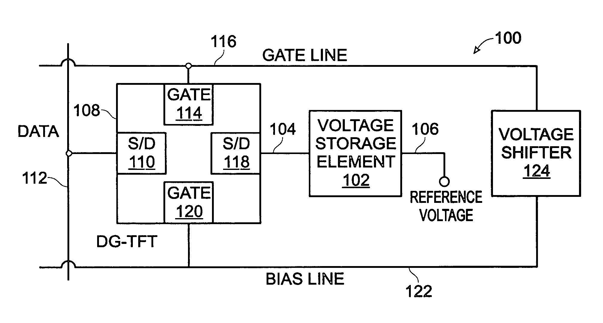
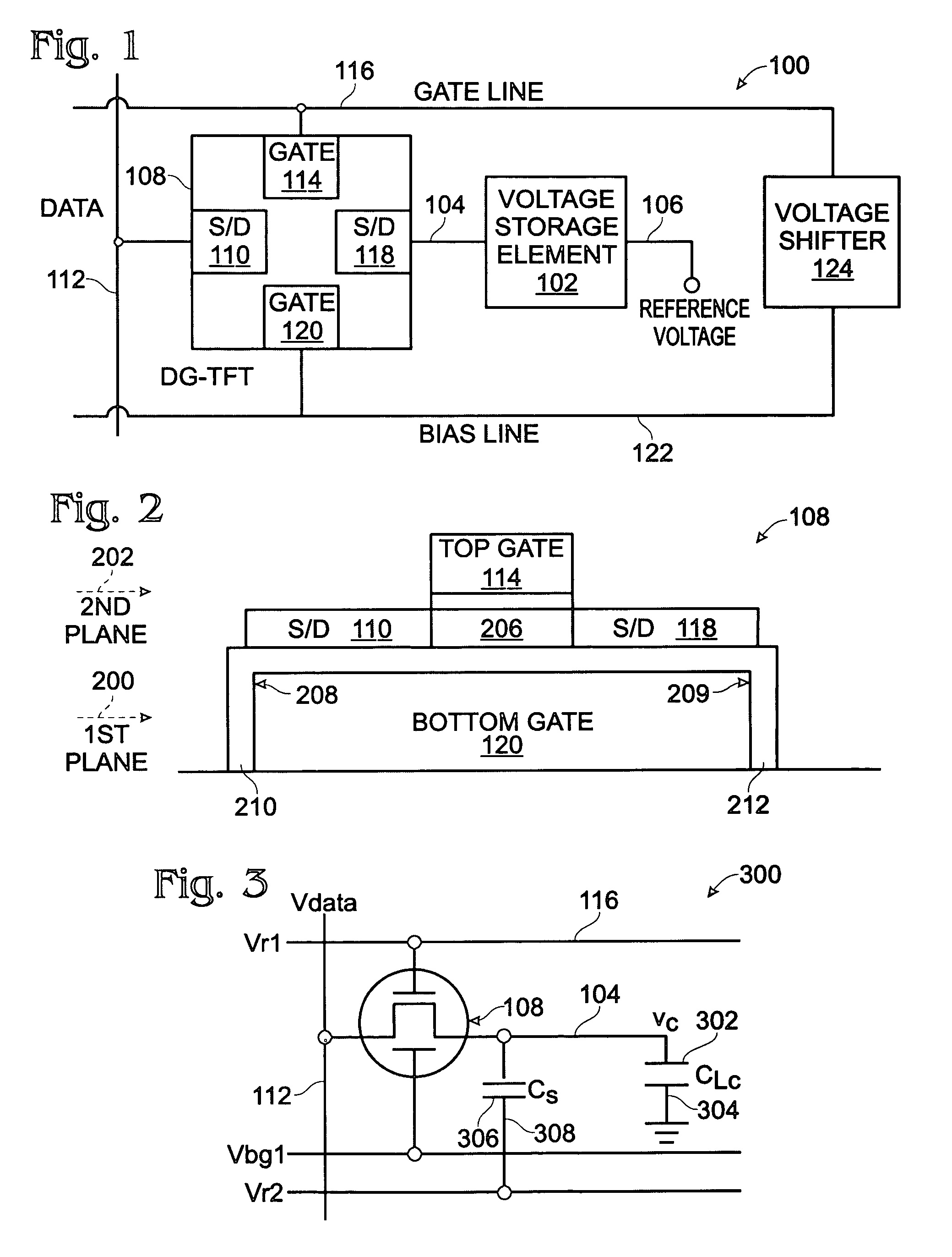
[0037]FIG. 1 is a schematic block diagram of a dual-gate thin-film transistor (DG-TFT) voltage storage circuit. The circuit 100 comprises a voltage storage element 102 having an input on line 104 and an output on line 106. A DG-TFT 108 has a first source / drain (S / D) 110 connected to a data line 112, a top gate 114 connected to a first gate line 116, a second S / D region 118 connected to the voltage storage element input 102 on line 104, and a bottom gate 120 connected to a bias line 122. The output of storage element 102 is shown as connected to a reference voltage (i.e., ground) on line 106.

[0038]FIG. 2 is a partial cross-sectional view of an exemplary DG-TFT. The DG-TFT 108 has the DG-TFT bottom gate 120 aligned in a first horizontal plane 200. The first S / D region 110 and second S / D region 118 are aligned in a second horizontal plane 202, overlying the first plane 200. The top gate 114 is aligned in a third horizontal plane 204, overlying the second plane 202. A channel region 20...


PUM


Abstract

A dual-gate thin-film transistor (DG-TFT) voltage storage circuit is provided. The circuit includes a voltage storage element, a DG-TFT having a first source / drain (S / D) connected to a data line, a top gate connected to a first gate line, a second S / D region connected to the voltage storage element, and a bottom gate connected to a bias line. In one aspect, the circuit further includes a voltage shifter having an input connected to the first gate line and an output to supply a bias voltage on the bias line. Examples of a voltage storage element include a capacitor, a liquid crystal (LC) pixel, and a light emitting diode (LED) pixel.

Description

RELATED APPLICATIONS [0001] This application is a continuation-in-part of a pending patent application entitled, DUAL-GATE THIN-FILM TRANSISTOR, invented by Scheule et al., Ser. No. 10 / 953,913, filed Sep. 28, 2004. This application is incorporated herein by reference.BACKGROUND OF THE INVENTION [0002] 1. Field of the Invention [0003] This invention generally relates to integrated circuit (IC) and liquid crystal display (LCD) fabrication and, more particularly, to a display with pixel elements controlled using a dual-gate thin-film transistor (DG-TFT). [0004] 2. Description of the Related Art [0005] In order to achieve high contrast and minimize crosstalk in a display system, such as a liquid display or a light-emitting diode panel, it is important to employ an active matrix (AM) architecture, where one or more active devices are used in each pixel to control the pixel switching characteristics. Various AM architectures exist, varying in complexity and principles of operation. Genera...

Claims


Application Information

Patent Timeline
Patent Type & Authority Applications(United States)
IPC IPC(8): G09G3/20
CPCG09G3/20G09G3/3208H01L29/78648G09G2300/08G09G2310/0262G09G3/3659
Inventor AFENTAKIS, THEMISTOKLESVOUTSAS, APOSTOLOS T.SCHUELE, PAUL J.
Owner SHARP KK
Why Eureka
Try Eureka