Liquid crystal display panel and manufacturing method thereof

a technology manufacturing method, which is applied in the direction of instruments, non-linear optics, optics, etc., can solve the problems of increased sealing width, abnormal display or premature failure, and increased width of sealant, so as to improve reliability and display quality of liquid crystal display panel, the effect of increasing the bonding stability

Active Publication Date: 2006-03-30
NYTELL SOFTWARE LLC
View PDF1 Cites 21 Cited by
  • Summary
  • Abstract
  • Description
  • Claims
  • Application Information

AI Technical Summary

Benefits of technology

[0011] Accordingly, the present invention is directed to a liquid crystal display panel having a thin film transistor array substrate and a color filter substrate. Spacers are disposed inside the liquid crystal display panel lean against the edge of structures having a step height above the surface of the thin film transistor array substrate. This increases the bonding stability between the color filter substrate and the thin film transistor array substrate so that the reliability and display quality of the liquid crystal display panel is improved.

Problems solved by technology

Although the conventional cathode ray tube (CRT) has high display quality and relatively low production cost, the electron gun inside the CRT not only produces hazardous radiation but also renders it bulky.
However, these ball spacers 150 within the liquid crystal display panel tend to gather in one place when the liquid crystal display panel is shake.
Because of the weight of a large substrate and the acoustic vibration produced by the speaker, the color filter substrate and the thin film transistor array substrate may separate from each other once the sealant reaches an aging or fatigue limit or the spacers are uneven.
This often leads to an abnormal display or a premature failure.
Although the problem can be ameliorated by increasing the width of the sealant so that the upper and lower substrate are more firmly sealed together, the additional width in the sealant often inconveniences production (coating and hardening) and panel edge narrowing.

Method used


Image

  • Liquid crystal display panel and manufacturing method thereof
  • Liquid crystal display panel and manufacturing method thereof
  • Liquid crystal display panel and manufacturing method thereof

Examples


Embodiment Construction

[0028] Reference will now be made in detail to the present preferred embodiments of the invention, examples of which are illustrated in the accompanying drawings. Wherever possible, the same reference numbers are used in the drawings and the description to refer to the same or like parts.

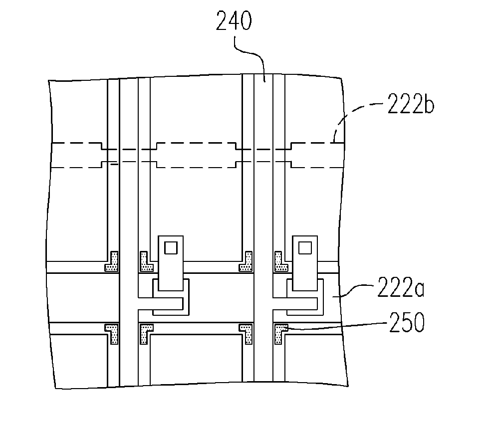
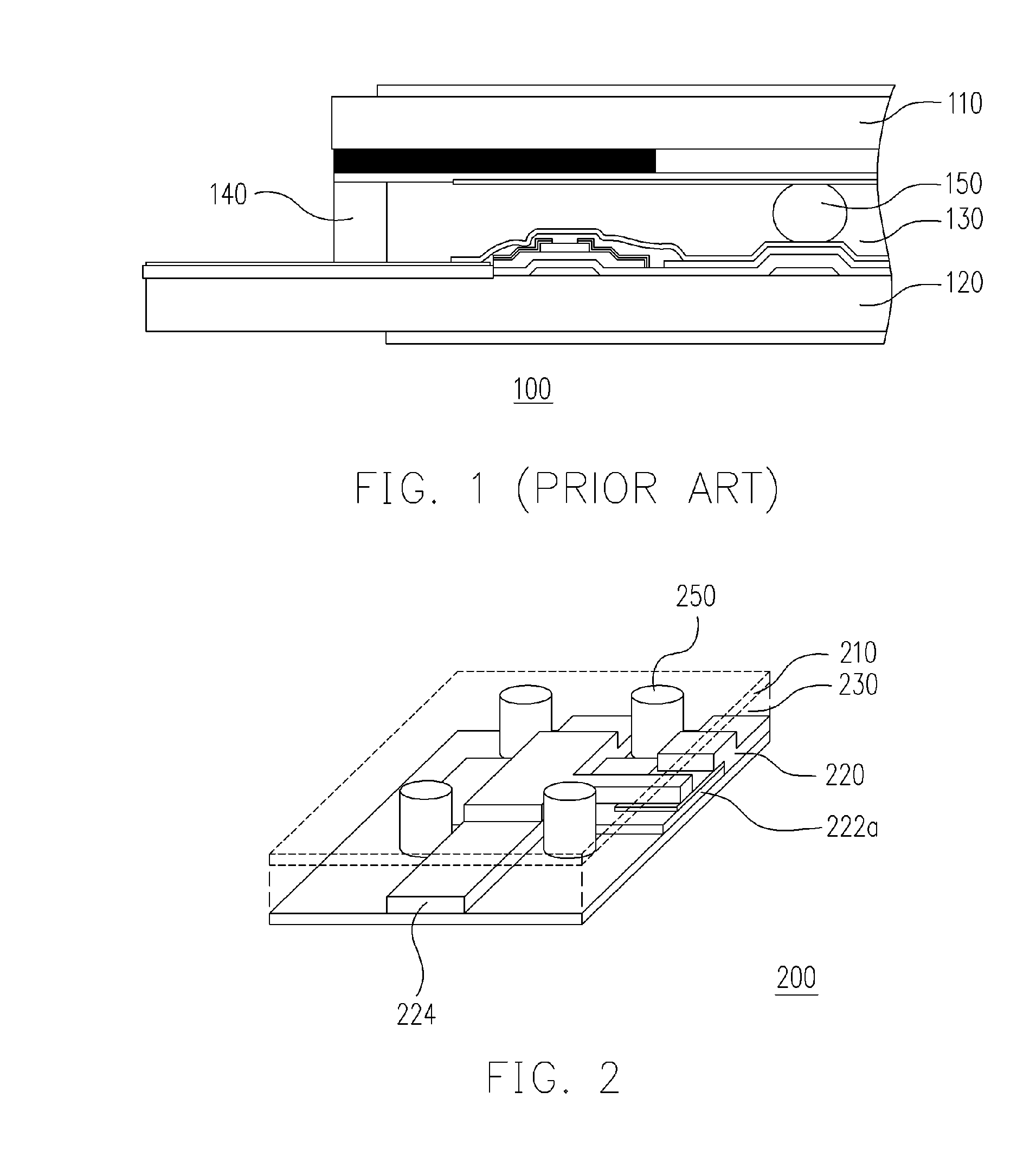
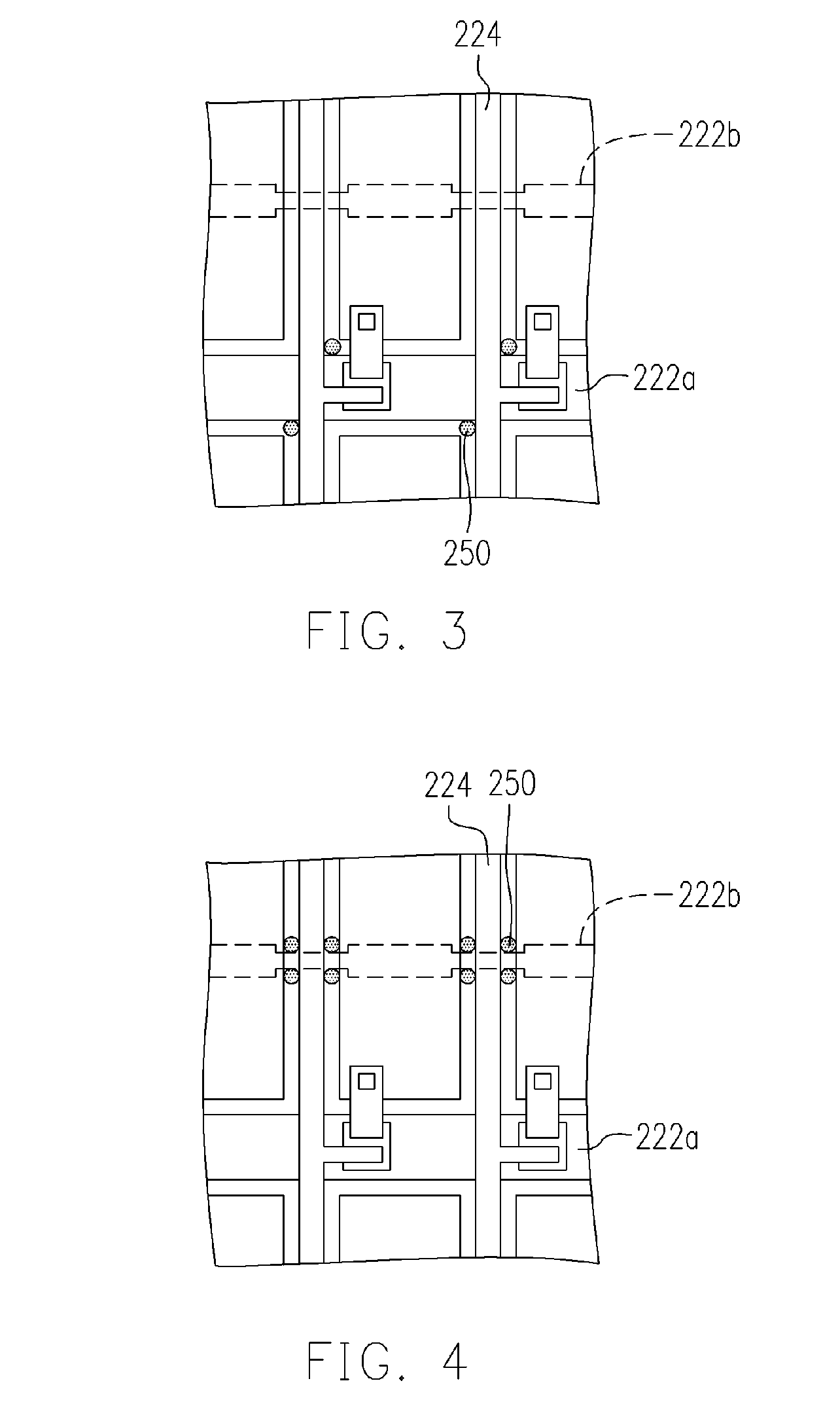
[0029]FIG. 2 is a perspective view of a section of a liquid crystal display panel according to one embodiment of the present invention. As shown in FIG. 2, the liquid crystal display panel 200 comprises a color filter substrate 210, a thin film transistor array substrate 220, a liquid crystal layer 230 and a plurality of spacers 250. The thin film transistor array substrate 200 has a plurality of gate layer lines and a plurality of source layer lines thereon. In one embodiment, the gate layer lines include scan lines 222a, and the source layer lines include data lines 224, for example. In another preferred embodiment, the gate layer lines include scan lines 222a and common lines 224 (shown in FIG. ...


PUM

PropertyMeasurementUnit
areaaaaaaaaaaa
shapeaaaaaaaaaa
photosensitiveaaaaaaaaaa

Abstract

A liquid crystal display panel and a manufacturing method thereof. The liquid crystal display panel comprises a color filter substrate and a thin film transistor array substrate arranged in parallel and a liquid crystal layer between the substrates. In addition, several spacers are disposed on a black matrix of the color filter substrate. These spacers lean on the edge of at least one of the gate layer lines and source layer lines on the thin film transistor array substrate. The invention increases the bonding stability between the color filter substrate and the thin film transistor array substrate so that the reliability and display quality of the liquid crystal display panel is improved.

Description

BACKGROUND OF THE INVENTION [0001] 1. Field of the Invention [0002] The present invention relates to a display panel and manufacturing method thereof. More particularly, the present invention relates to a high reliability liquid crystal display panel and manufacturing method thereof. [0003] 2. Description of Related Art [0004] With the rapid development of multi-media systems, image data is mostly transmitted in a digital format through a network rather than in an analogue format through a cable. To match the life style of modern people, lighter and compact video or image display devices are also being designed. Although the conventional cathode ray tube (CRT) has high display quality and relatively low production cost, the electron gun inside the CRT not only produces hazardous radiation but also renders it bulky. [0005] With recent advance in opto-electronic fabricating techniques and the maturity of semiconductor manufacturing processes, the development of flat panel display devi...

Claims


Application Information

Patent Timeline
Patent Type & Authority Applications(United States)
IPC IPC(8): G02F1/1339
CPCG02F1/136286G02F1/13394
Inventor LIU, MENG-CHICHEN, HSIAO-FEN
Owner NYTELL SOFTWARE LLC
Why Eureka
Try Eureka