Read head having shaped read sensor-biasing layer junctions using partial milling and method of fabrication

Inactive Publication Date: 2006-03-30
HITACHI GLOBAL STORAGE TECH NETHERLANDS BV
View PDF40 Cites 10 Cited by
  • Summary
  • Abstract
  • Description
  • Claims
  • Application Information

AI Technical Summary

Benefits of technology

[0016] It is another advantage of the present invention that manufacturing yields are improved since there are less yield losses due to shorting between the sensor and the bottom shield.
[0017] It is yet another advantage of the present invention that the amount of material removed is less, and therefore there is less redeposited material that gets thrown against the sensor, thus producing cleaner junctions, with potentially lower junction resistance.
[0018] It is a further advantage of the present invention that the total mill time is shorter, and thus there is less chance of Electrostatic Discharge (ESD) damage.
[0019] It is a yet further advantage of the present invention that since the metal is not completely removed during a partial mill, islands of material are not left behind (unlike in the full mill case, where at the end of the milling process, there are islands of patterned material): rather, there is a continuous film of material on the wafer at

Problems solved by technology

However, the limits of this technique are being reached because with trackwidths less than 130 nm, the width of the photoresist lower layer 44 becomes too small to support the upper layer 42.
It is very desirable to vary the junction profile, and thus to affect the sharpness of the free layer edges, sharpness of the pinned layer edges, and the material on which the hard bias layers are grown, hence affecting device performance.
It has been discovered that there are several disadvantages to this “complete milling” and many advantages to a “partial milling” operation in which some layers of sensor stack are left behind after the patterning operation, retaining a thin layer of material which covers the dielectric layer.
In particular, when using complete milling, the thin dielectric layer underneath the sensor may b

Method used


Image

  • Read head having shaped read sensor-biasing layer junctions using partial milling and method of fabrication
  • Read head having shaped read sensor-biasing layer junctions using partial milling and method of fabrication
  • Read head having shaped read sensor-biasing layer junctions using partial milling and method of fabrication

Examples


Example

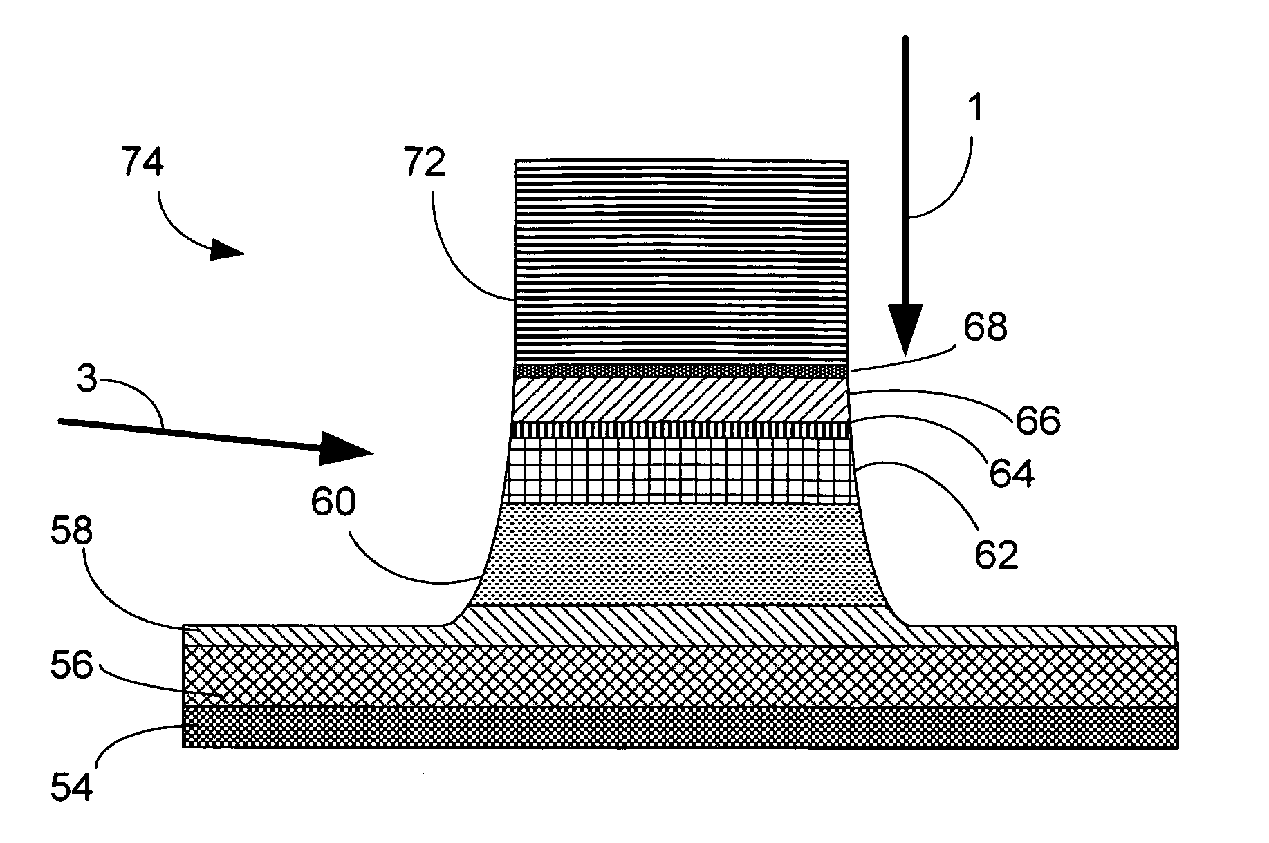
[0032] The present invention is a disk drive read head having partial milling of the sensor layers above the dielectric layer, and a method for producing this read head.

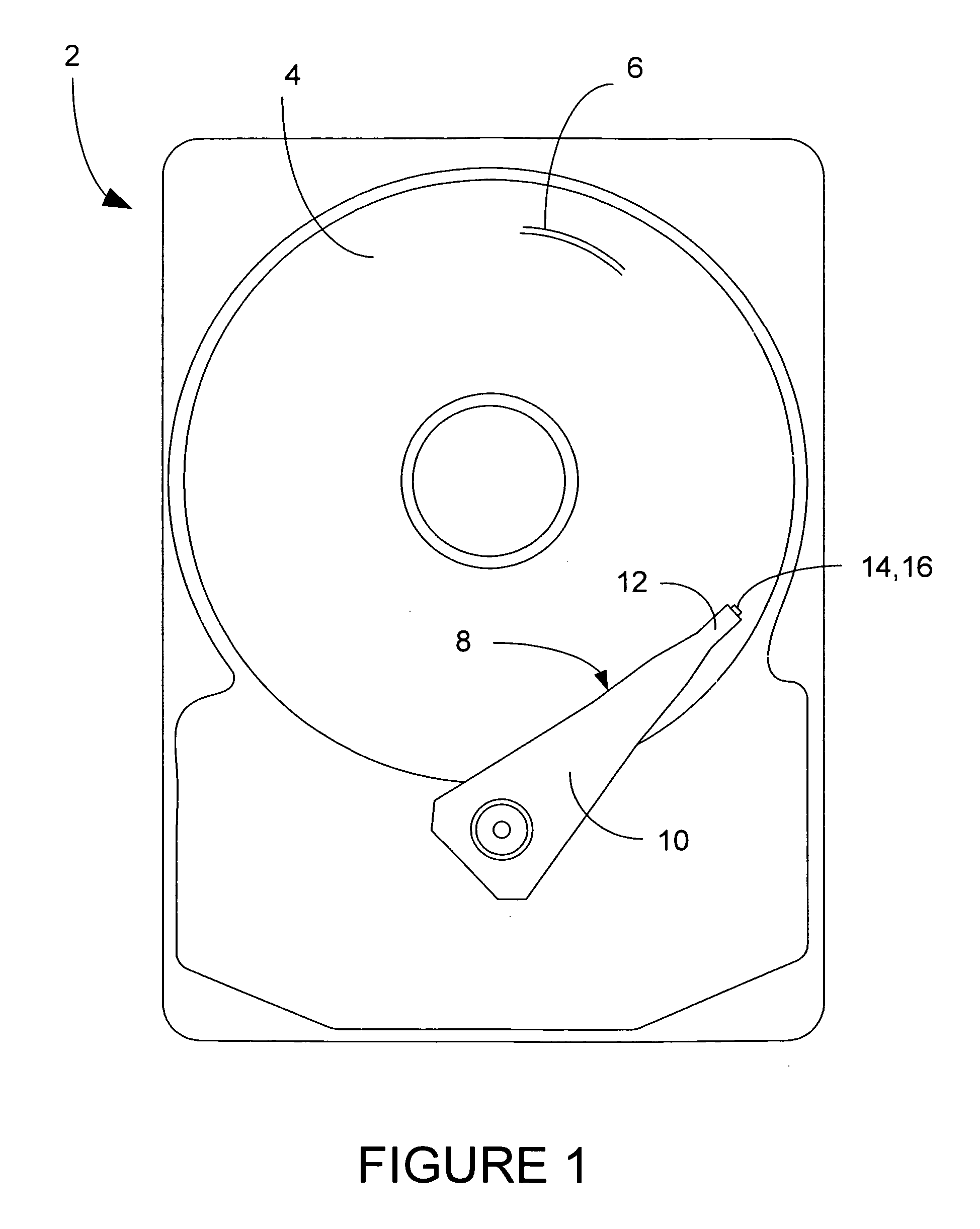
[0033] A hard disk drive 2 is shown generally in FIG. 1, having one or more magnetic data storage disks 4, with data tracks 6 which are written and read by a data read / write device 8. The data read / write device 8 includes an actuator arm 10, and a suspension 12 which supports one or more magnetic heads 14 included in one or more sliders 16.

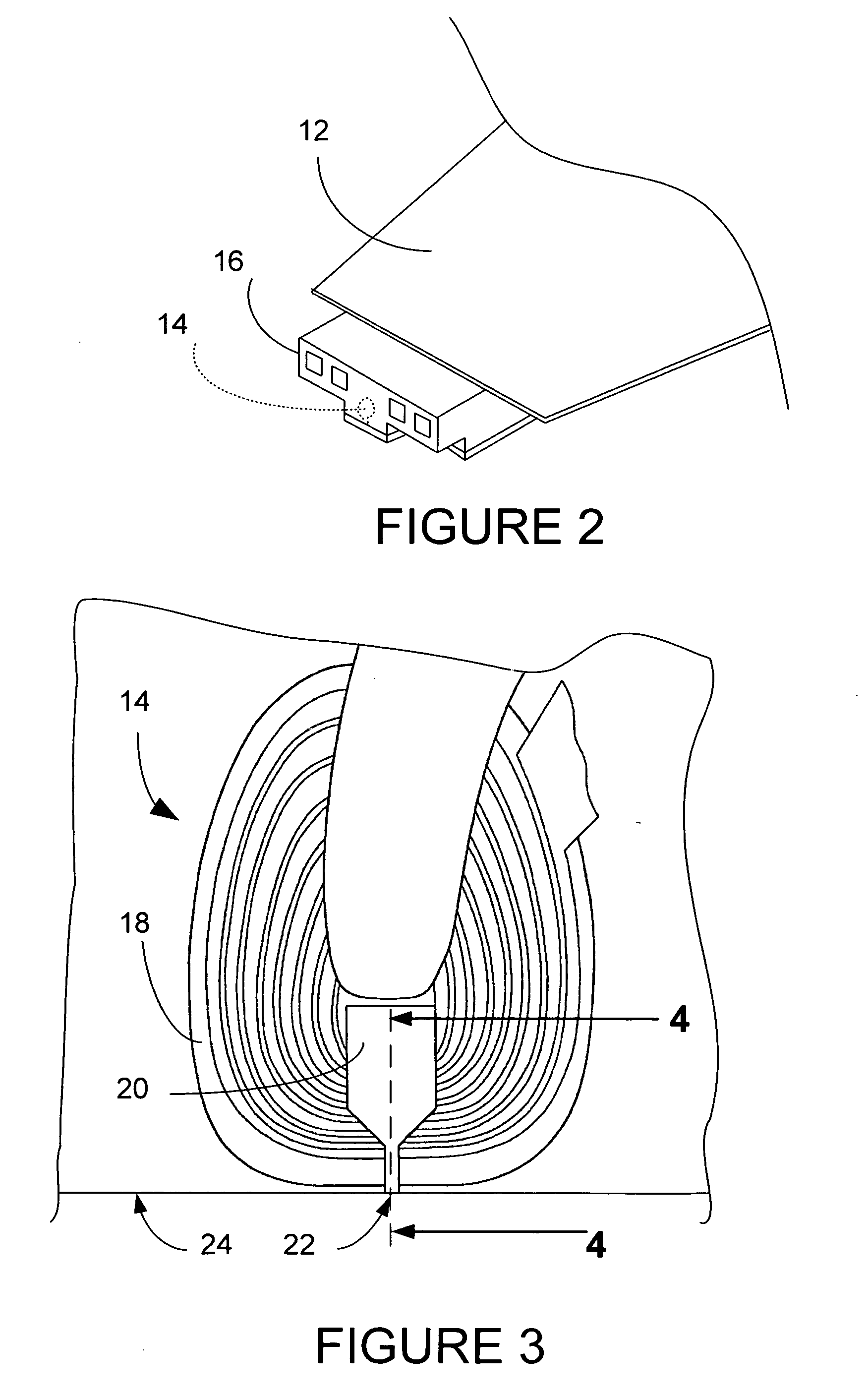
[0034]FIG. 2 shows a slider 16 in more detail being supported by suspension 12. The magnetic head 14 is shown in dashed lines, and in more detail in FIGS. 3 and 4. The magnetic head 14 includes a coil 18 and P1 pole, which also acts as S2 shield, thus making P1 / S220. P1 S2 may also be made as two discrete layers. The second pole P222 is separated from P1 / S2 by write gap 23.

[0035] The read sensor 50 is sandwiched between the first shield S130 and the second shield P1 / S220. There ...


PUM

PropertyMeasurementUnit
Angleaaaaaaaaaa
Structureaaaaaaaaaa
Depthaaaaaaaaaa

Abstract

A method is disclosed for fabricating a read head for a magnetic disk drive having a read head sensor and a hard bias layer, where the read head has a shaped junction between the read head sensor and the hard bias layer. The method includes providing a layered wafer stack to be shaped. A single- or multi-layered photoresist mask having no undercut is deposited upon the layered wafer stack to be shaped. The layered wafer stack is shaped by the output of a milling source, where the shaping includes partial milling to within a partial milling range to form a shaped junction. A hard bias layer is then deposited which is in contact with the shaped junction of the wafer stack. A read head and a magnetic hard disk drive having a read head layer stack which has been partially milled are also disclosed.

Description

BACKGROUND OF THE INVENTION [0001] 1. Field of the Invention [0002] The present invention relates generally to fabrication of electronic components, and more particularly, this invention relates to shaping of the junction between a hard biasing layer and the free layer of a magnetic read sensor of a hard disk drive. [0003] 2. Description of the Prior Art [0004] In recent years there has been a constant drive to increase the performance of hard disk drives by increasing the areal data storage density of the magnetic hard disk. This is done by reducing the written data track width, such that more tracks per inch can be written on the disk. This naturally requires that the width of the read head be reduced so magnetic field interference from adjacent data tracks is not picked up. Read sensors, of which one type is referred to as a “spin valve”, developed to read trackwidths smaller than 130 nm depends upon the ability to ion mill the sensor to these very small dimensions, and to reliab...

Claims


Application Information

Patent Timeline
IPC IPC(8): G11B5/33G11B5/127
CPCG11B5/3903G11B5/3932G11B5/398Y10T29/49044Y10T29/49041Y10T29/49052Y10T29/49039Y10T29/49046Y10T29/49043Y10T29/49048
Inventor CYRILLE, MARIE-CLAIREJAYASEKARA, WIPUL PEMSIRIPINARBASI, MUSTAFA MICHAEL
Owner HITACHI GLOBAL STORAGE TECH NETHERLANDS BV
Why Eureka
Try Eureka