

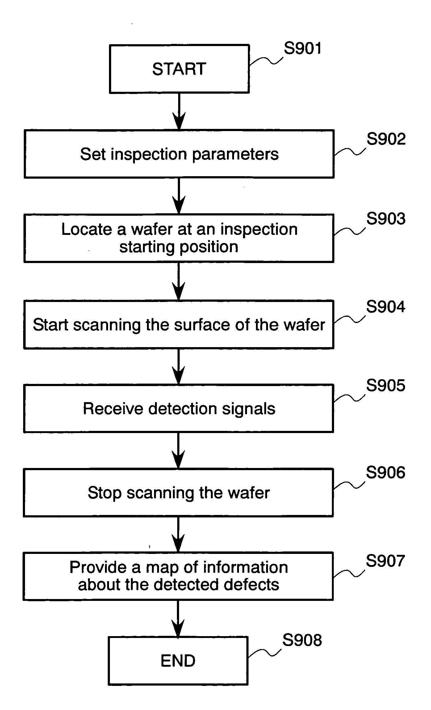
Method and apparatus for detecting defects
a technology of defect detection and method, applied in the direction of individual semiconductor device testing, semiconductor/solid-state device testing/measurement, instruments, etc., can solve the problem that the method cannot deal with the variation of the thickness of the inner layer, and achieve the effect of stable sensitivity
- Summary
- Abstract
- Description
- Claims
- Application Information
AI Technical Summary
Benefits of technology
Problems solved by technology
Method used
Image

Examples
Embodiment Construction
[0022] Preferred embodiments of the present invention will be described.
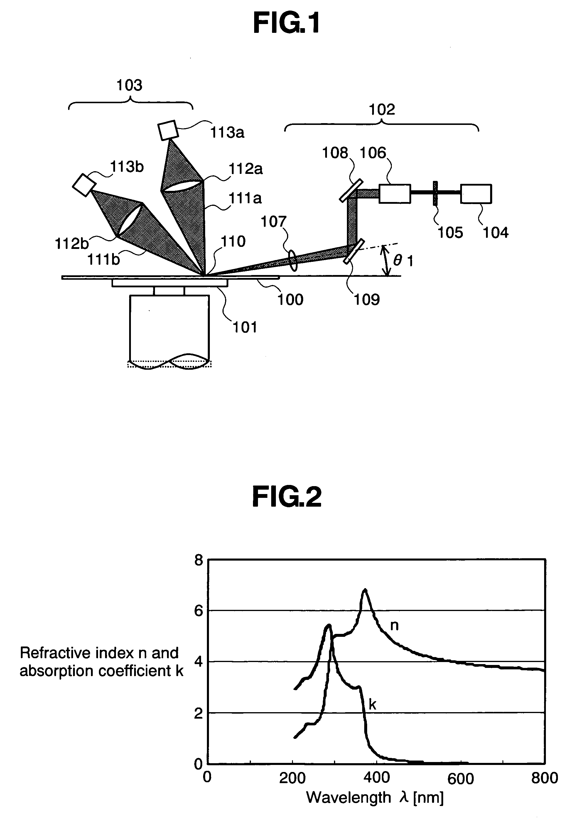
[0023]FIG. 1 shows an inspection apparatus which represents a preferred embodiment according to the present invention for inspecting a semiconductor wafer for foreign matter adhering thereto. The inspection apparatus includes, as principal components, a wafer stage 101, an illuminating optical system 102 and a detecting optical system 103. The illuminating optical system 102 includes a laser 104, such as an Ar laser or a semiconductor laser, a wave plate 105, a beam expander 106 and a condenser lens 107. The wave plate 105 adjusts the direction of polarization of a laser beam emitted by the laser 104 to an optional direction. The beam expander 106 increases the diameter of the laser beam. The laser beam gathered by the condenser lens 107 is projected on a wafer 100 to illuminate a detection area 110 on a wafer 100. Mirrors 108 and 109 are used, when necessary, to change the optical path of the laser beam.
[0024...
PUM
 Abstract
Description
Claims
Application Information