High voltage FET switch with conductivity modulation

a high-voltage, switch technology, applied in the direction of semiconductor devices, electrical equipment, basic electric elements, etc., can solve the problems of low specific on-resistance in sic-based devices, inability to meet the requirements of high-voltage switching, and high resistance. high-voltage, negligible switching loss

Active Publication Date: 2006-04-06
CALLAHAN CELLULAR L L C
View PDF2 Cites 33 Cited by
  • Summary
  • Abstract
  • Description
  • Claims
  • Application Information

AI Technical Summary

Benefits of technology

[0010] A high power field-effect transistor (FET) switch is presented which overcomes the problems noted above. The switch is particularly well-suited to high power switching applications, providing a very low on-resistance, a high blocking voltage, and negligible switching loss.

Problems solved by technology

However, on-resistance increases very rapidly when its breakdown voltage is increased.
This makes the on-state power losses unacceptable where high DC supply voltages are used.
This allows much higher doping and a much thinner drift layer for a given blocking voltage, resulting in a very low specific on-resistance in SiC-based devices.
Unfortunately, many SiC devices developed to date exhibit severe commercialization constraints.
These demands result in a complex fabrication process which is unsuitable for large-scale manufacturing.
However, the IGBT has disadvantages which render it unsuitable for some applications.
Another drawback to IGBTs is that they can “latch-up”, at which point they are no longer under the control of the gate voltage.
When in this mode, conduction through the device can no longer be controlled by the gate voltage.

Method used


Image

  • High voltage FET switch with conductivity modulation
  • High voltage FET switch with conductivity modulation
  • High voltage FET switch with conductivity modulation

Examples


Embodiment Construction

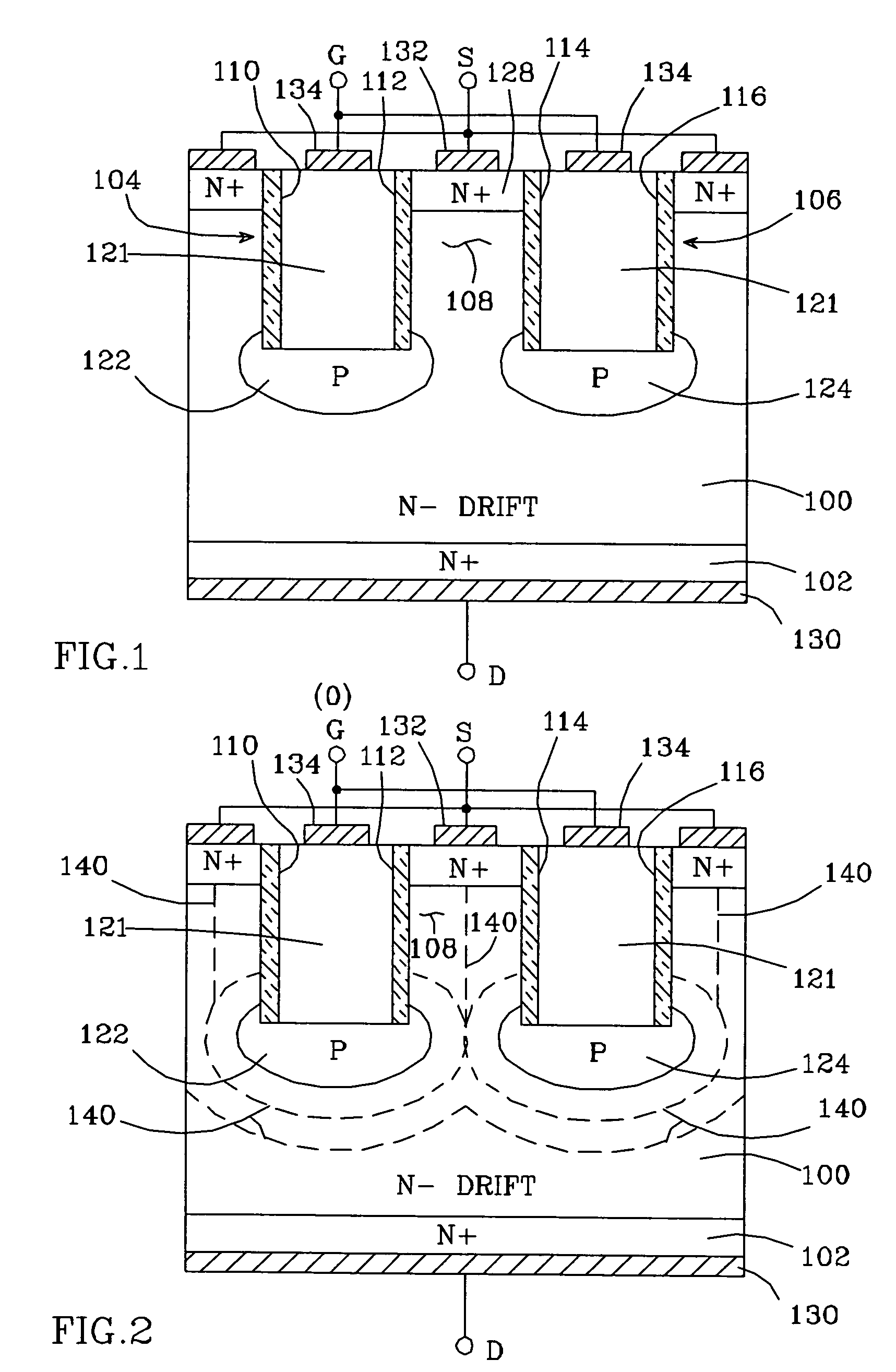
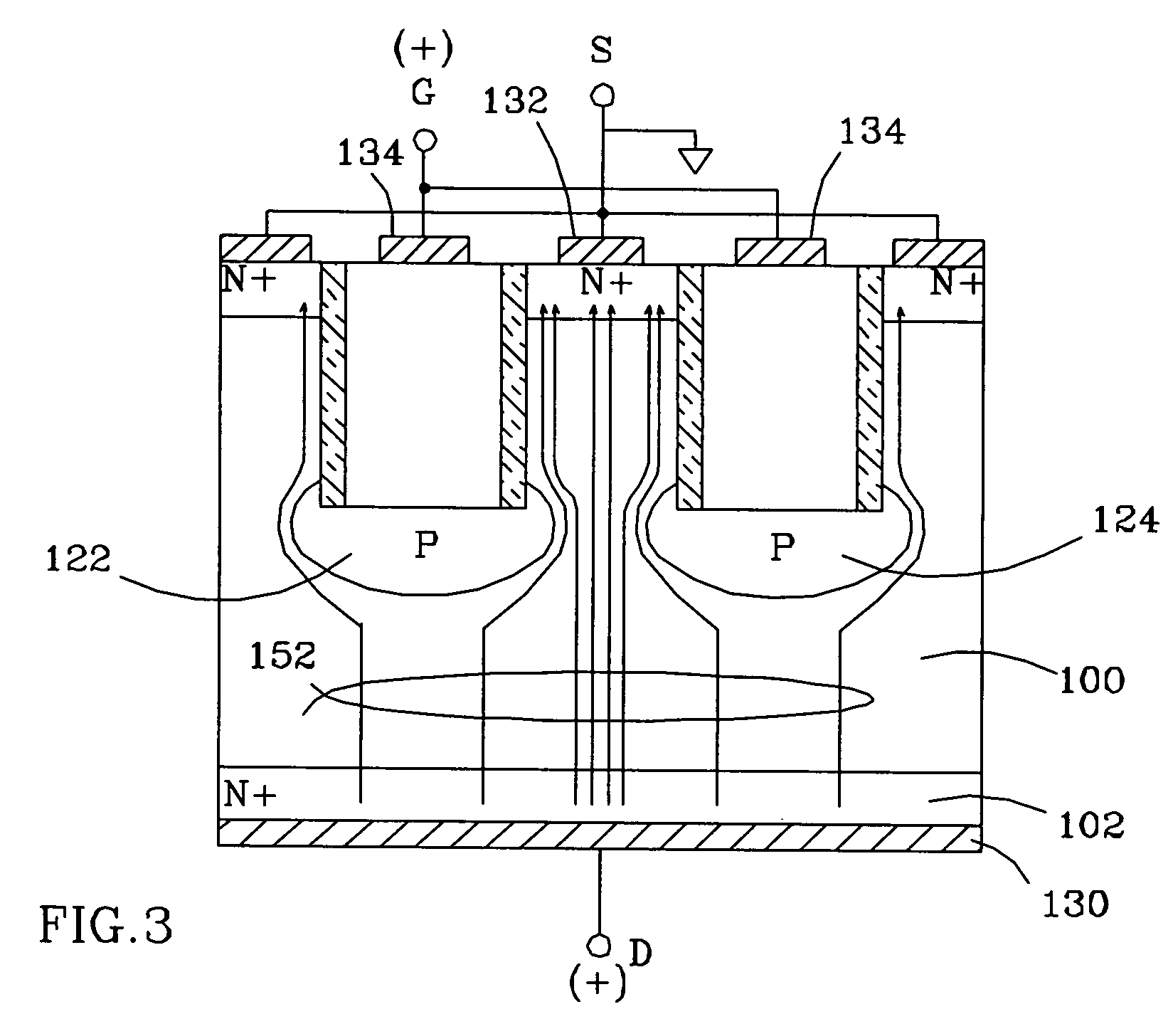
[0027] An exemplary embodiment of a FET switch in accordance with the present invention is shown in FIG. 1. A N− drift layer 100 of a desired thickness is on a first N+ layer 102. Recessed into drift layer 100 opposite the N+ layer are a pair of trenches 104, 106, which are separated by a mesa region 108 comprised of that portion of the N− drift layer found between the trenches. The trenches are recessed to a predetermined depth, with the depth defining each trench's “bottom”. Each trench has oxide side-walls 110, 112, 114, 116, and is filled with a conductive material 121. At the bottom of each trench is a shallow P region 122, 124, which extends across the bottom and around the corners of each trench's side-walls into the drift layer. A second N+ layer 128 is on N− drift layer 100 within mesa region 108.

[0028] The first N+ layer 102 provides an ohmic contact to drift layer 100, and a first layer of metal 130 on N+ layer 102 provides a drain connection for the FET switch. The seco...


PUM


Abstract

A high power FET switch comprises an N− drift layer, in which pairs of trenches are recessed to a predetermined depth; oxide side-walls extend to the trench bottoms, and each trench is filled with a conductive material. N+ and metal layers on opposite sides of the drift layer provide drain and source connections for the FET, and the conductive material in each trench is connected together to provide a gate connection. A shallow P region extends across the bottom and around the corners of each trench's side-walls into the drift layer. The application of a sufficient gate voltage causes holes to be injected from the shallow P regions into the N− drift layer, thereby modulating the drift layer's conductivity and lowering the device's on-resistance, and enabling current to flow between the drain and source connections.

Description

BACKGROUND OF THE INVENTION [0001] 1. Field of the Invention [0002] This invention relates to the field of high power semiconductor switches. [0003] 2. Description of the Related Art [0004] Semiconductor devices are increasingly required to accommodate high currents and / or high voltages without failing. Many high power applications call for the use of a semiconductor switch which is required to conduct a large current when turned on, and to block a high voltage when off. [0005] One device used in such applications is the power metal-oxide-semiconductor field-effect transistor (MOSFET). As discussed in J. Baliga, Power Semiconductor Devices, PWS Publishing Co. (1996) at p. 426, a power MOSFET exhibits excellent fast switching capability and safe-operating-area. When designed to block relatively low voltages (less than 200 volts), the power MOSFET has a low on-resistance. However, on-resistance increases very rapidly when its breakdown voltage is increased. This makes the on-state pow...

Claims


Application Information

Patent Timeline
Patent Type & Authority Applications(United States)
IPC IPC(8): H01L29/00
CPCH01L29/7722H01L29/8083
Inventor CHANG, HSUEH-RONG
Owner CALLAHAN CELLULAR L L C
Why Eureka
Try Eureka