Diamond substrate formation for electronic assemblies

a technology of semiconductor substrates and electronic assemblies, applied in the direction of semiconductor devices, semiconductor/solid-state device details, electrical devices, etc., can solve the problems of exponential growth of leakage current and significant increase of leakage curren

Inactive Publication Date: 2006-04-06
INTEL CORP
View PDF42 Cites 23 Cited by
  • Summary
  • Abstract
  • Description
  • Claims
  • Application Information

AI Technical Summary

Problems solved by technology

Elevated temperatures can result in significantly larger leakage current...

Method used


Image

  • Diamond substrate formation for electronic assemblies
  • Diamond substrate formation for electronic assemblies
  • Diamond substrate formation for electronic assemblies

Examples


Embodiment Construction

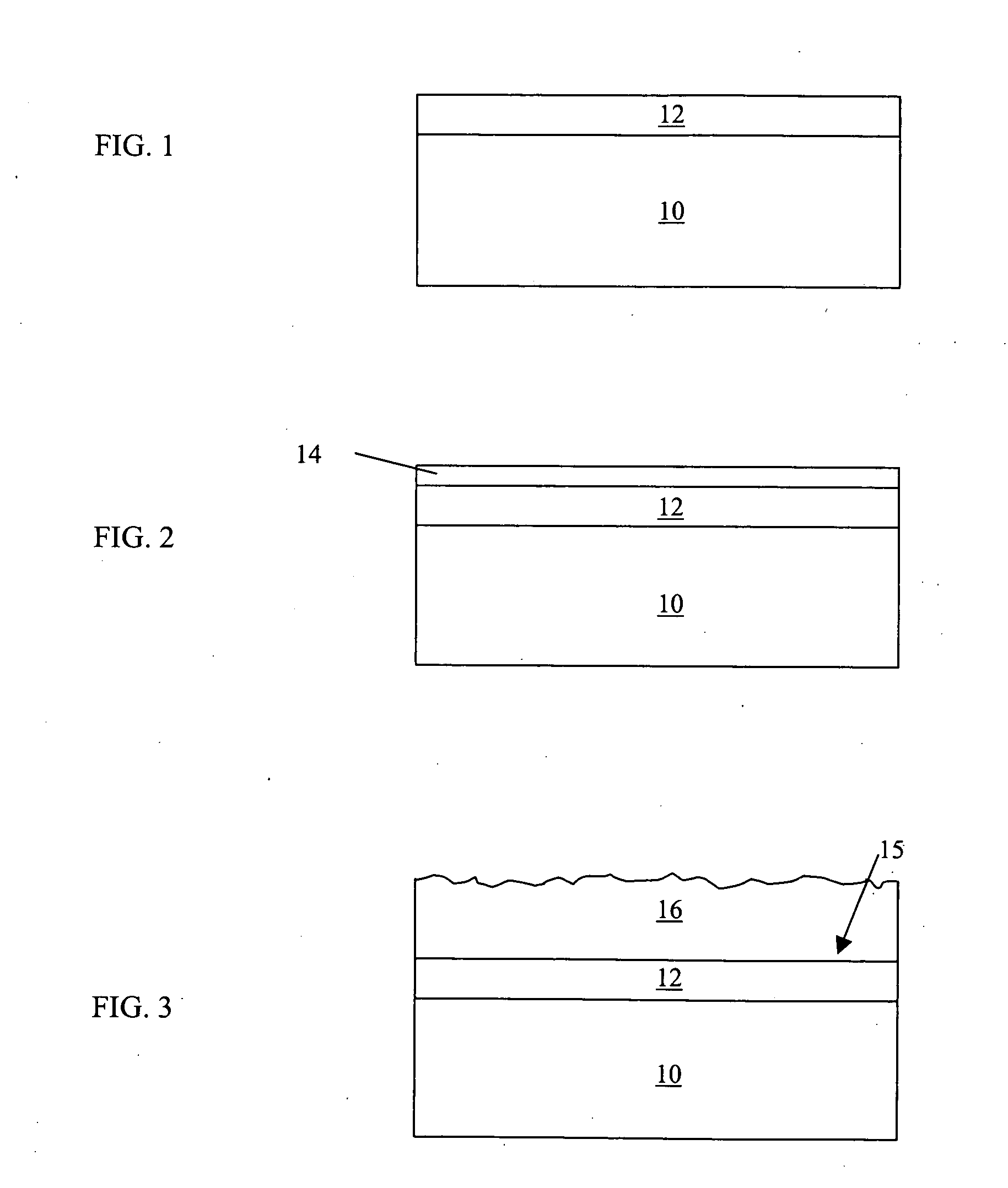
[0014] Certain embodiments relate to the formation of an assembly including a diamond substrate having a thin semiconductor layer thereon. Diamond is an advantageous material for thermal performance because it has a substantially higher thermal conductivity than copper or silicon. Diamond layers have been grown on silicon substrates. However, such diamond layers often have a high degree of warpage and thus are not suitable for the fabrication of devices such as transistors. Such warpage may be at least in part due to the thermal expansion mismatch between the silicon substrate and the diamond. The process for forming such a diamond layer requires relatively high temperatures and as such, the stresses developed due to the thermal expansion mismatch are substantial.

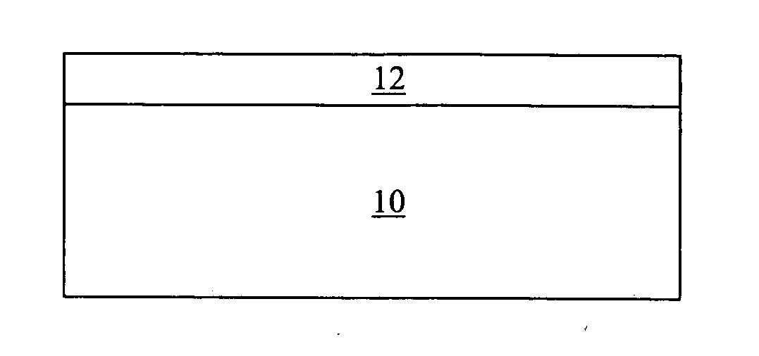
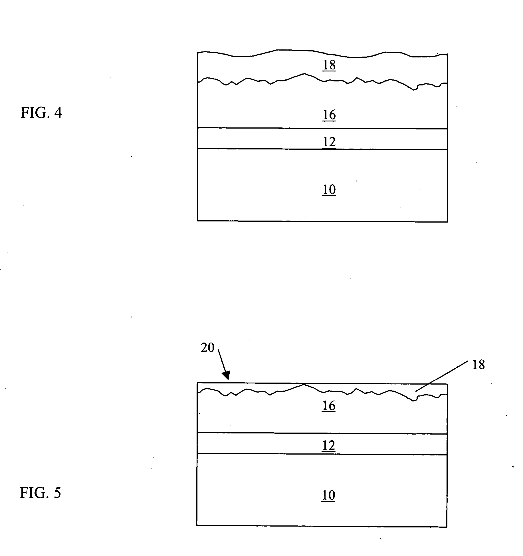
[0015]FIGS. 1-3 illustrate a first embodiment of the present invention. As seen in FIG. 1, a layer 12 is formed on a diamond support substrate 10. The layer 12 is preferably a porous layer of material that can withstand re...


PUM

PropertyMeasurementUnit
Temperatureaaaaaaaaaa
Lengthaaaaaaaaaa
Fractionaaaaaaaaaa

Abstract

Electronic assemblies and methods for forming assemblies including a diamond substrate are described. One embodiment includes providing a diamond support and forming a porous layer of SiO2 on the diamond support. A diamond layer is formed by chemical vapor deposition on the porous layer so that the porous layer is between the diamond support and the diamond layer. A polycrystalline silicon layer is formed on the diamond layer. The polycrystalline silicon layer is polished to form a planarized surface. A semiconductor layer is coupled to the polysilicon layer. After coupling the semiconductor layer to the polysilicon layer, the diamond support is detached from the diamond layer by breaking the porous layer. The semiconductor layer on the diamond layer substrate is then further processed to form a semiconductor device.

Description

RELATED ART [0001] Electronic devices typically include integrated circuits formed on semiconductor materials such as silicon. Semiconductor wafers may be processed to form various electronic devices having integrated circuits and diced into bulk semiconductor chips. Silicon-on-insulator (SOI) structures have been developed as an alternative to bulk silicon device technology. In general, SOI fabrication processes result in increased packing densities, improved performances, better device isolations and reduced extrinsic parasitic elements, particularly those of the source and drain as well as leakage currents and thus significantly speeding up circuit operations. SOI substrates generally include a thin layer of silicon on top of an insulator, wherein circuit components are formed in and on the thin layer of silicon. The insulator can be formed from a variety of materials such as silicon oxide and sapphire. [0002] As device integration increases, integrated circuits require cooling t...

Claims


Application Information

Patent Timeline
IPC IPC(8): H01L21/50
CPCH01L21/76259H01L23/3732H01L2924/0002Y10S148/012H01L2924/00
Inventor HU, CHUANCHRYSLER, GREGORY M.LU, DAOQIANG
Owner INTEL CORP
Why Eureka
Try Eureka