Low-k dielectric material based upon carbon nanotubes and methods of forming such low-k dielectric materials

a carbon nanotube and low-k dielectric technology, applied in the field of dielectric materials, can solve the problems of cross-talk noise, limited circuit performance and functional capability of circuit elements, and limited integration of low-k dielectrics into damascene processes

Active Publication Date: 2006-04-06
GLOBALFOUNDRIES US INC
View PDF22 Cites 34 Cited by
  • Summary
  • Abstract
  • Description
  • Claims
  • Application Information

AI Technical Summary

Benefits of technology

[0008] In accordance with an embodiment of the invention, a dielectric material for forming a structure of an integrated circuit is comprised of a plurality of carbon nanostructures, such as carbon nanotubes or carbon buckyballs. In one embodiment of the invention, the nanostructures forming the dielectric material may be fluorinated. In another embodiment of the invention, the dielectric material may have a dielectric constant less than about three (3). The dielectric material may be used to form a dielectric layer in a semiconductor structure that includes at least one conductive feature electrically isolated from nearby conductive features by portions of the dielectric layer.

Problems solved by technology

Circuit performance and functional capability of the circuit elements are eventually limited by the signal-transmission effectiveness and efficiency of the BEOL interconnect structure.
The reduction in line-to-line spacing serves to increase the line-to-line capacitance, which causes propagation delay by slowing the speed of the signals carried by the metallization lines, and results in cross talk noise.
Damascene processes place stringent requirements on the properties of the candidate low-k dielectric materials, which has limited the integration of low-k dielectrics into damascene processes.
After manufacture, BEOL interconnect structures formed using organic dielectric materials have experienced significant reliability problems resulting from mismatches in the thermal coefficient of expansion with neighboring inorganic materials.

Method used


Image

  • Low-k dielectric material based upon carbon nanotubes and methods of forming such low-k dielectric materials
  • Low-k dielectric material based upon carbon nanotubes and methods of forming such low-k dielectric materials
  • Low-k dielectric material based upon carbon nanotubes and methods of forming such low-k dielectric materials

Examples


Embodiment Construction

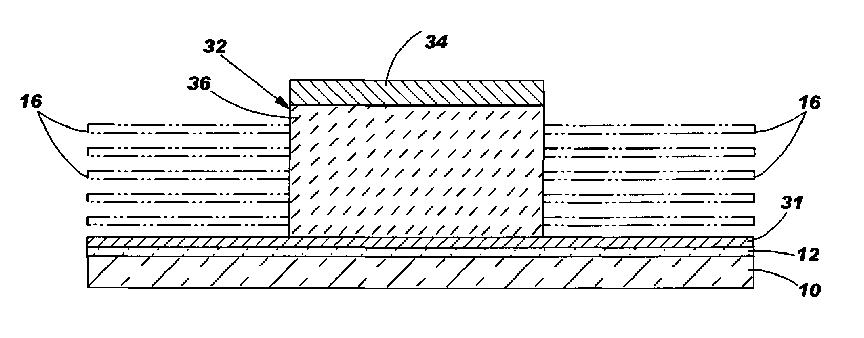
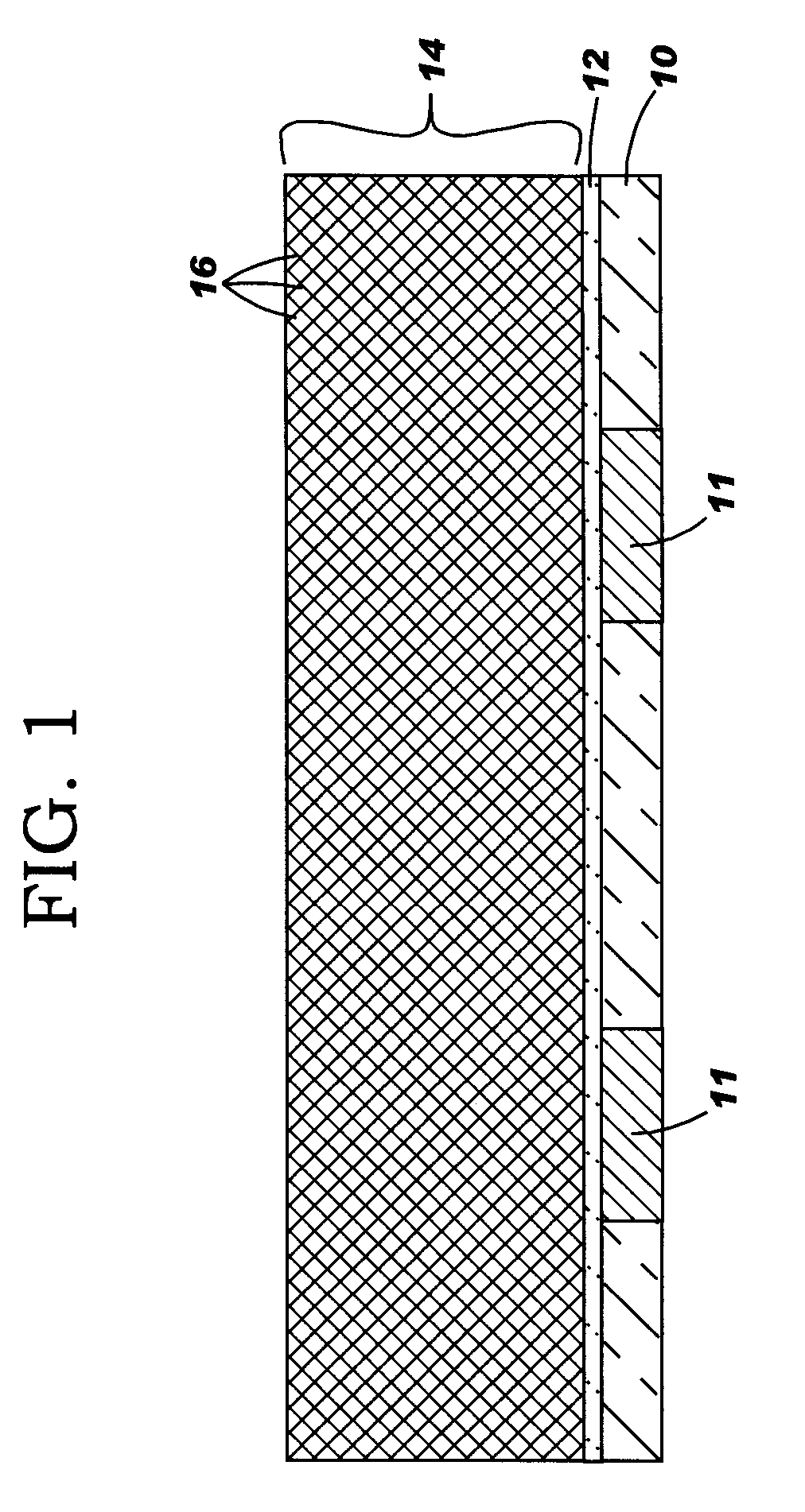
[0018] With reference to FIG. 1, a substrate 10 is covered by a layer 12 of a suitable cap material, such as silicon nitride (Si3N4). Substrate 10 contains features 11 that are to be contacted, like a silicon diffusion region (e.g., a source or drain for a semiconductor device) or an underlying wiring or metallization structure. Substrate 10 may be a semiconductor wafer composed of any semiconductor material including, but not limited to, silicon (Si), silicon germanium (SiGe), silicon-on-insulator, and other like Si-containing semiconductor materials. The substrate 10 may be doped with either n-type or p-type impurities, depending on the desired device or circuit element to be fabricated, and may contain various isolation and / or device regions either formed in the substrate 10 or on a surface thereof. Substrate 10 may also be one of the interconnect levels of a multilevel interconnect structure, a dielectric material, a buried barrier layer, a metallization line, or another substra...


PUM

PropertyMeasurementUnit
dielectric constantaaaaaaaaaa
temperatureaaaaaaaaaa
dielectric constantaaaaaaaaaa

Abstract

A low-k dielectric material for use in the manufacture of semiconductor devices, semiconductor structures using the low-k dielectric material, and methods of forming such dielectric materials and fabricating such structures. The low-k dielectric material comprises carbon nanostructures, like carbon nanotubes or carbon buckyballs, that are characterized by an insulating electronic state. The carbon nanostructures may be converted to the insulating electronic state either before or after a layer containing the carbon nanostructures is formed on a substrate. One approach for converting the carbon nanostructures to the insulating electronic state is fluorination.

Description

FIELD OF THE INVENTION [0001] The invention relates generally to semiconductor materials, structures, devices, and fabrication methods and, more particularly, to dielectric materials for forming a structure for an integrated circuit, structures formed with the dielectric materials, and methods for forming such dielectric materials and structures. [0002] BACKGROUND OF THE INVENTION [0003] Progressive miniaturization of feature sizes in circuit elements has improved the performance and increased the functional capability of integrated circuits (IC's). Back-end-of-line (BEOL) multilevel interconnect structures have been developed that complement advances in circuit element density realized by size reductions by more effectively routing signal paths between the constituent circuit elements of the IC. Circuit performance and functional capability of the circuit elements are eventually limited by the signal-transmission effectiveness and efficiency of the BEOL interconnect structure. Dama...

Claims


Application Information

Patent Timeline
Patent Type & Authority Applications(United States)
IPC IPC(8): H01L21/28
CPCB82Y10/00H01L21/3146H01L21/3185H01L21/76814H01L21/7682H01L21/76826H01L21/76831H01L21/76888H01L2221/1047H01L21/02115H01L21/02282
Inventor FURUKAWA, TOSHIHARUHAKEY, MARK CHARLESHOLMES, STEVEN JOHNHORAK, DAVID VACLAVKOBURGER, CHARLES WILLIAM III
Owner GLOBALFOUNDRIES US INC
Why Eureka
Try Eureka